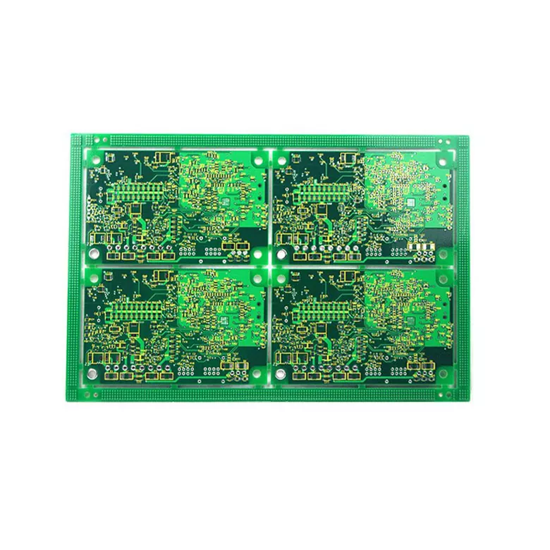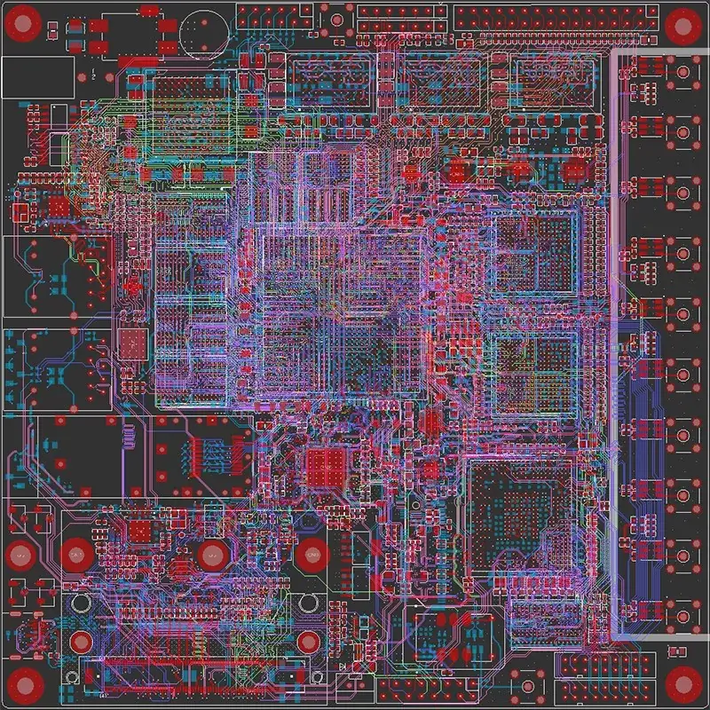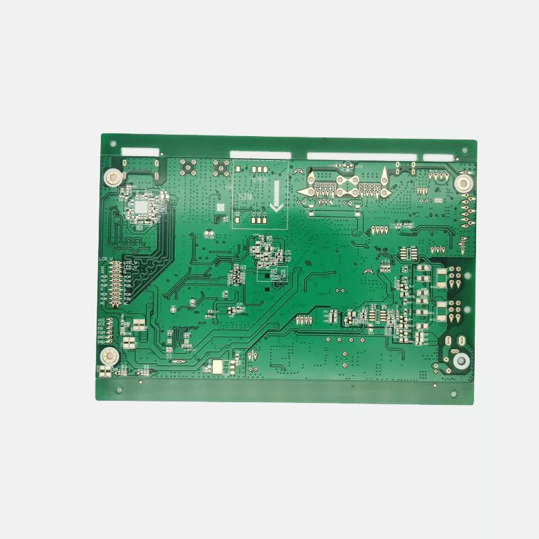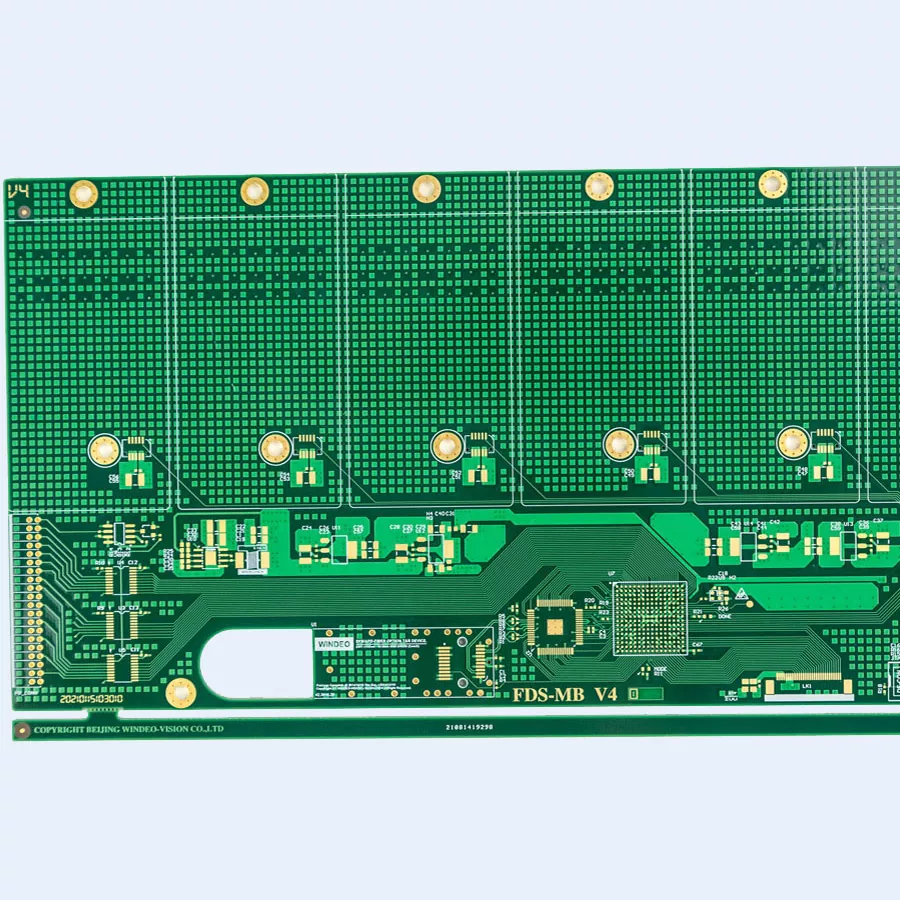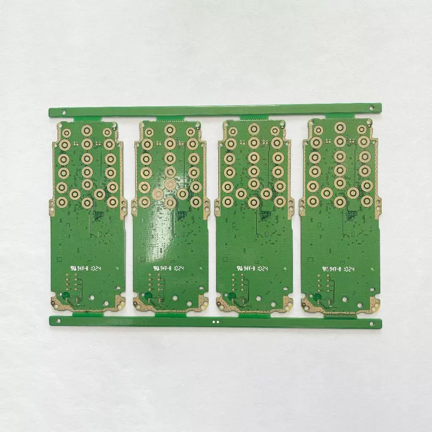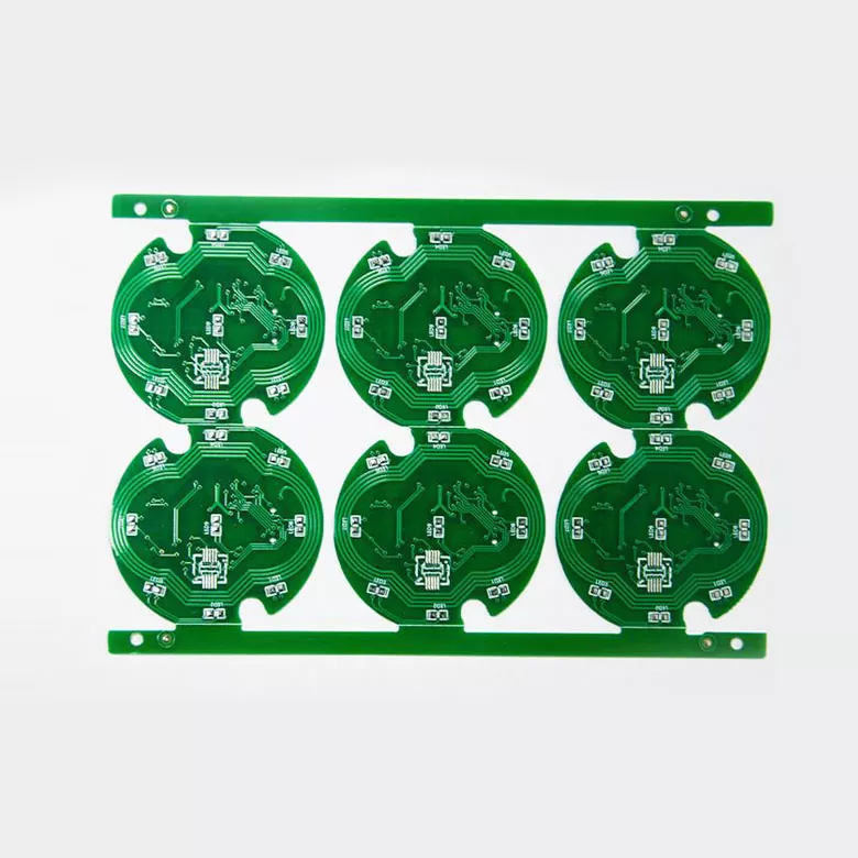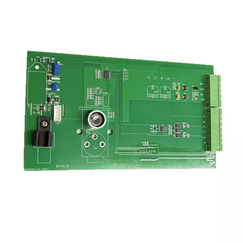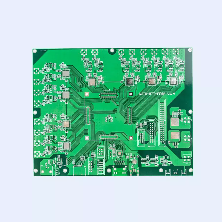

When modern electronic equipment demands accurate power conversion, dependable signal routing, and compact circuit integration, choosing the right Converter and Selector PCB becomes essential. Aisen provides customized PCB manufacturing solutions designed to support complex electrical architectures, high-density layouts, multilayer construction, and demanding industrial applications.
A Converter and Selector PCB is more than a platform for mounting electronic components. It provides the electrical and mechanical foundation for systems that need power conversion, signal selection, signal routing, or a combination of these functions. As electronic devices become more compact and sophisticated, PCB performance directly affects electrical stability, signal integrity, thermal management, and long-term reliability.
Table of Contents
- What Is a Converter and Selector PCB?
- Why Is PCB Design Important for Conversion and Selection?
- What Features Should a High-Performance PCB Have?
- What Are the Key Converter and Selector PCB Specifications?
- Where Are Converter and Selector PCBs Used?
- How Is a Converter and Selector PCB Manufactured?
- How Can PCB Quality and Reliability Be Ensured?
- How Should You Choose a PCB Manufacturer?
- Frequently Asked Questions
- Why Work With an Experienced PCB Partner?
What Is a Converter and Selector PCB?
A Converter and Selector PCB is a printed circuit board designed to support electrical conversion, signal selection, signal switching, or signal routing within an electronic system. Depending on the application, the board may be responsible for transferring electrical power between different voltage levels, managing multiple signal channels, or coordinating different functional circuits.
Converter circuits can be found in power supplies, industrial control equipment, energy systems, communication devices, and many other electronic products. Selector functions are equally important when equipment needs to choose between multiple inputs, outputs, channels, or operating modes.
The PCB therefore needs to provide a reliable physical structure while maintaining appropriate electrical characteristics. Layer configuration, copper thickness, trace width, impedance, via technology, dielectric materials, surface finish, and thermal design all influence the final performance of the board.
- Power conversion: Supports circuits that transform electrical power between different voltage or current conditions.
- Signal selection: Allows electronic systems to select specific signal channels or circuit paths.
- Signal routing: Connects different functional areas while maintaining required electrical characteristics.
- Thermal management: Helps dissipate heat generated by power components.
- System integration: Allows multiple electronic functions to be incorporated into a compact assembly.
Why Is PCB Design Important for Conversion and Selection?
Conversion and selection circuits often operate under different electrical conditions. A power converter may require substantial current capacity and effective heat dissipation, while a high-speed selector may require precise routing and impedance control. The PCB must therefore be designed according to the actual operating environment rather than treated as a generic circuit carrier.
Electrical Stability
Appropriate copper thickness and trace geometry help manage current flow and reduce unnecessary electrical losses. For sensitive circuits, careful grounding and routing can also help minimize unwanted interference.
Signal Integrity
High-speed signals can be affected by trace geometry, dielectric properties, layer structure, and impedance variation. A properly engineered multilayer PCB can provide dedicated signal and reference layers that improve routing consistency.
Thermal Performance
Power conversion components may generate considerable heat during continuous operation. Copper areas, thermal vias, component positioning, and suitable board materials can contribute to better heat management.
Compact Integration
Modern electronic products increasingly require smaller circuit assemblies. Multilayer and HDI technologies allow more electrical connections to be integrated into a limited board area without simply increasing the external dimensions.
Manufacturing Reliability
A technically advanced PCB design is only valuable when it can be manufactured consistently. Design-for-manufacturing considerations should therefore be incorporated before production begins.
What Features Should a High-Performance PCB Have?
The ideal Converter and Selector PCB depends on the application, but several capabilities are particularly valuable for demanding projects.
- Multilayer construction: Provides additional routing space and allows power, ground, and signal layers to be organized efficiently.
- High copper thickness: Helps support applications involving higher current loads.
- Fine-line technology: Enables dense circuit layouts and compact component arrangements.
- Controlled impedance: Helps maintain predictable electrical performance for high-speed signal transmission.
- HDI capability: Supports miniaturized electronic products requiring high routing density.
- Microvia technology: Creates additional routing options in advanced multilayer designs.
- Multiple surface finishes: Allows the board finish to be selected according to assembly and application requirements.
- Precision drilling: Supports accurate via structures and multilayer interconnections.
For complex projects, these capabilities should be evaluated together. A board with excellent routing density but insufficient current capacity, for example, may not be appropriate for a power conversion application.
What Are the Key Converter and Selector PCB Specifications?
Technical specifications provide an important reference when comparing PCB suppliers. The following parameters represent capabilities suitable for a wide range of advanced Converter and Selector PCB projects.
| Specification | Capability | Why It Matters |
|---|---|---|
| Layer Count | 1–32 layers | Supports designs ranging from simple boards to highly complex multilayer circuits. |
| Board Thickness | 0.3–5.0 mm | Provides flexibility for different mechanical and installation requirements. |
| Copper Thickness | Up to 6 oz | Provides options for applications requiring higher current-carrying capability. |
| Minimum Line Width | 0.076 mm / 3 mil | Supports high-density routing and compact PCB layouts. |
| Impedance Control | ±10%, with ±8% available | Useful for high-speed and sensitive signal applications. |
| Minimum Microvia | 0.1 mm | Supports advanced HDI and high-density interconnection designs. |
| Controlled Depth Drilling | ±0.1 mm | Helps achieve accurate blind and buried via structures. |
| Surface Finish | ENIG, OSP, HASL and other options | Allows the finish to be matched with assembly and application requirements. |
These specifications should be treated as a starting point rather than a universal configuration. The correct layer count, copper weight, material, impedance structure, and board thickness should always be determined according to the electrical design and operating environment.
Where Are Converter and Selector PCBs Used?
The combination of conversion and selection functions makes these PCBs suitable for many electronic systems. Their applications can range from power management to industrial automation and communication equipment.
Power Electronics
- DC-DC converter systems
- AC-DC power supply equipment
- Power management modules
- Energy storage systems
- Solar power equipment
Industrial Automation
- Industrial control systems
- Process control equipment
- Signal switching systems
- Automation interfaces
- Electronic control cabinets
Communication and Networking
- Signal selection modules
- Network switching equipment
- Communication interfaces
- Signal conversion systems
- Data routing equipment
Consumer and Specialized Electronics
Compact Converter and Selector PCBs can also be integrated into specialized electronic devices where limited installation space requires a high level of circuit integration.
How Is a Converter and Selector PCB Manufactured?
High-quality PCB manufacturing requires close control from engineering review through final inspection. This becomes particularly important for multilayer boards, fine-line structures, HDI designs, and high-current applications.
A typical manufacturing workflow includes the following stages:
- Engineering review: Analyze the PCB files and confirm electrical and manufacturing requirements.
- Material preparation: Select and inspect suitable laminate, copper foil, solder mask, and other materials.
- Inner-layer fabrication: Transfer and form the required internal circuit patterns.
- Lamination: Combine the multilayer structure under controlled temperature and pressure.
- Precision drilling: Create through holes, blind vias, buried vias, or microvias as required.
- Copper plating: Establish reliable electrical connections between PCB layers.
- Outer-layer processing: Form the final external circuit pattern.
- Surface finishing: Apply the specified surface treatment.
- Automated inspection: Detect potential manufacturing defects.
- Electrical testing: Verify circuit continuity and electrical integrity before shipment.
Aisen's manufacturing information describes a multilayer production process with numerous controlled stages, supported by automated optical inspection, electrical testing, and reliability verification. Such process control is particularly important when the PCB will be integrated into equipment expected to operate continuously.
How Can PCB Quality and Reliability Be Ensured?
PCB quality should be evaluated through both process control and finished-product testing. Visual inspection alone cannot identify every electrical or internal structural problem, particularly on complex multilayer boards.
A reliable quality-control system can include:
- Incoming material inspection to verify raw material consistency.
- AOI inspection to identify circuit pattern defects during production.
- Dimensional inspection to confirm critical mechanical tolerances.
- Electrical testing to verify continuity and circuit integrity.
- Reliability testing to evaluate performance under defined conditions.
- Final inspection to ensure finished boards meet customer specifications.
For procurement teams, it is also useful to examine a supplier's ability to maintain consistent quality from prototype quantities to mass production. A manufacturer that understands both engineering requirements and production control can help reduce the risk of unexpected variation during scale-up.
How Should You Choose a PCB Manufacturer?
Choosing a PCB manufacturer should involve more than comparing the lowest quotation. For a technically demanding Converter and Selector PCB, engineering support, manufacturing capabilities, quality management, delivery performance, and communication can have a direct impact on project success.
Before selecting a China PCB supplier or manufacturer, procurement teams should evaluate:
- Available PCB layer count and board thickness range
- Maximum copper thickness
- Minimum trace width and spacing
- Controlled impedance capabilities
- HDI and microvia manufacturing experience
- Available surface finishes
- Prototype and small-batch production capability
- Mass-production capacity
- AOI and electrical testing procedures
- Engineering and DFM support
- Production lead times and communication efficiency
Another important factor is whether the supplier can provide technical feedback before production. Early identification of potential problems involving trace width, stack-up, thermal management, drill design, or component spacing can prevent costly redesigns later.
For this reason, the best supplier is not necessarily the one offering the lowest initial price. Instead, look for a manufacturing partner that can provide a balanced combination of technical expertise, production consistency, quality assurance, and responsive service.
Frequently Asked Questions
What does a Converter and Selector PCB do?
A Converter and Selector PCB supports electronic functions such as power conversion, signal conversion, signal selection, and signal routing. Its exact configuration depends on the electrical architecture and application requirements.
Can a Converter and Selector PCB be customized?
Yes. PCB dimensions, layer count, copper thickness, materials, impedance structure, via technology, surface finish, and other characteristics can be customized according to the customer's design requirements.
How many layers are suitable for a converter PCB?
There is no universal layer count. Simple converter circuits may use fewer layers, while complex power and signal systems may require multilayer construction to provide adequate routing, grounding, power distribution, and thermal performance.
Why is copper thickness important?
Copper thickness influences the board's current-carrying capability and electrical resistance. Higher copper weights can be useful when a PCB needs to handle relatively high currents or manage heat generated by power circuits.
Is impedance control necessary for selector PCBs?
It can be essential when the selector circuit handles high-speed or sensitive signals. Controlled trace geometry, appropriate stack-up design, and stable dielectric characteristics help maintain predictable signal transmission.
Can HDI technology be used for Converter and Selector PCBs?
Yes. HDI technology can be used when a project requires high routing density, compact dimensions, fine-pitch components, or advanced interconnection structures. Microvias and other HDI techniques can provide additional routing flexibility.
What should I provide when requesting a PCB quotation?
Ideally, provide Gerber files or complete PCB design files, board dimensions, layer count, material requirements, copper thickness, surface finish, impedance requirements, quantity, testing requirements, and any special application conditions. Providing complete information helps the manufacturer prepare a more accurate quotation and production plan.
Why Work With an Experienced PCB Partner?
A reliable Converter and Selector PCB requires a combination of appropriate circuit architecture, suitable materials, precise manufacturing, effective quality control, and application-focused engineering. Whether you are developing a high-current converter, a signal selector, an industrial control board, or a compact multilayer electronic assembly, choosing the right manufacturing partner can help improve reliability while reducing development and production risks.
If you are looking for a customized PCB solution with flexible layer configurations, high-density routing, controlled impedance, advanced manufacturing capabilities, and professional engineering support, contact us to discuss your requirements. Aisen can work with your specifications to develop a Converter and Selector PCB solution that matches your electrical, mechanical, quality, and production objectives.