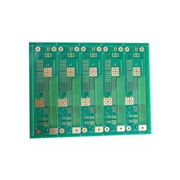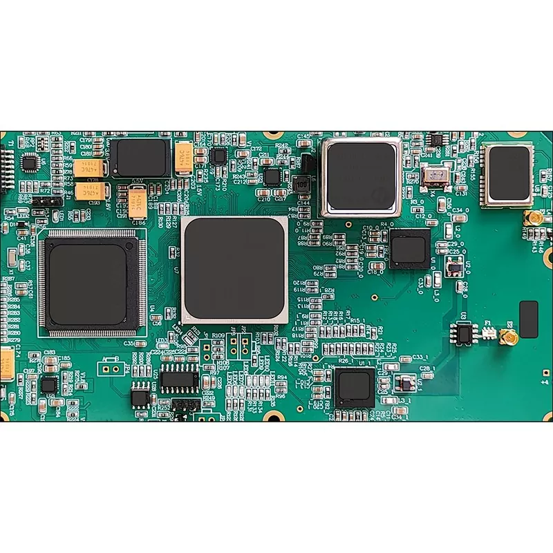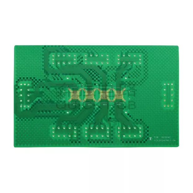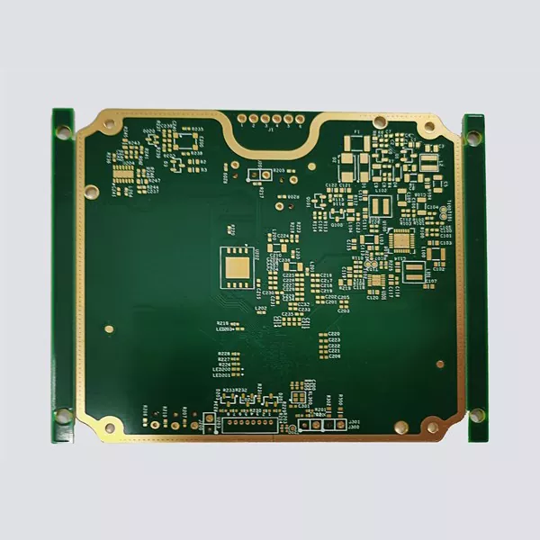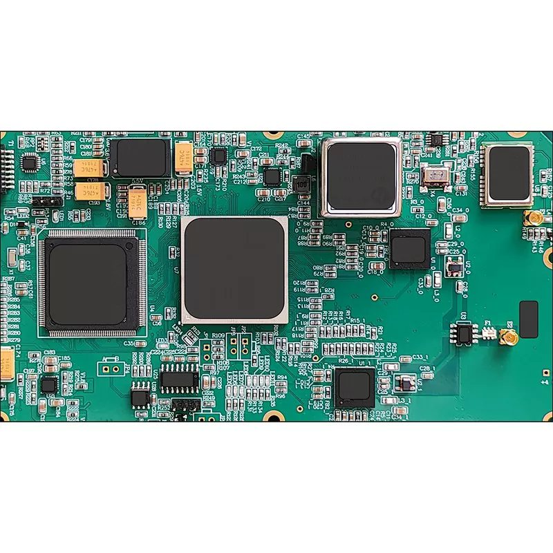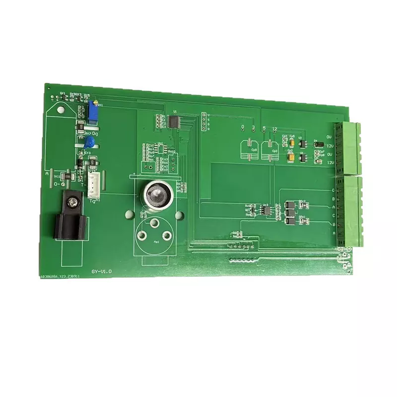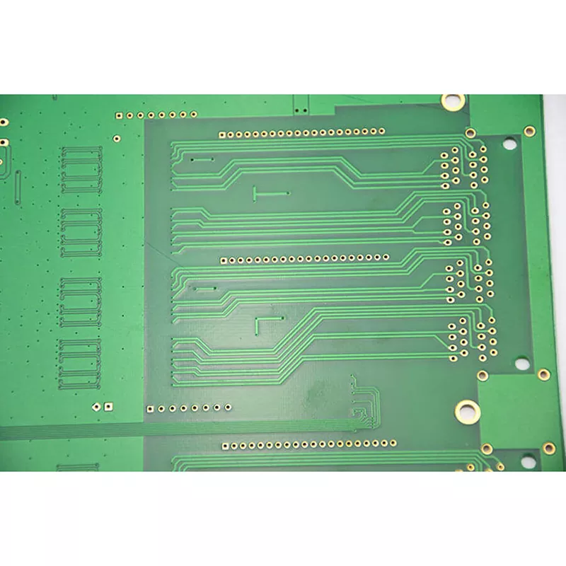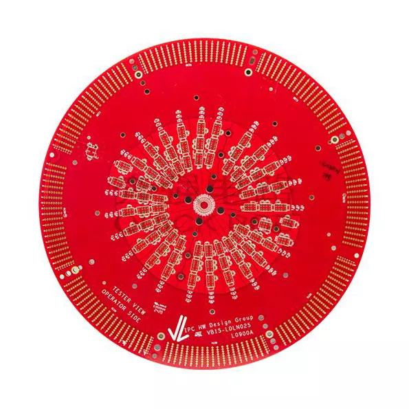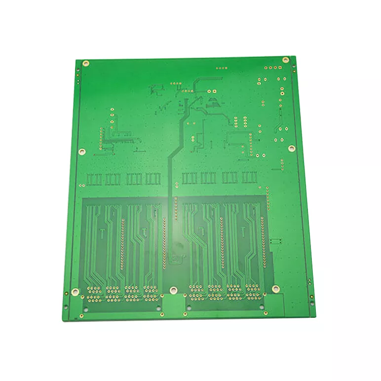

Aisen develops precision PCB solutions for electrical measurement applications where signal integrity, thermal stability, and manufacturing consistency directly affect instrument performance. An Electrical Measuring Instruments PCB is more than a circuit carrier—it supports the accurate acquisition, conditioning, processing, and transmission of electrical signals in demanding measurement equipment.
From digital multimeters and oscilloscopes to power analyzers and industrial monitoring systems, modern instruments depend on carefully engineered PCB structures. Proper routing, grounding, material selection, layer configuration, and inspection can help reduce interference and maintain repeatable electrical performance.
Electrical measurement equipment must process signals accurately under different operating conditions. This makes PCB design and manufacturing particularly important. A precision measurement PCB should address noise control, signal integrity, thermal stability, circuit isolation, impedance management, and production consistency. Aisen provides customized PCB solutions supporting 2–32 layers, minimum 3mil/3mil line width and spacing, via accuracy of ±0.05mm, impedance control of ±8%, and copper thickness up to 6oz. These capabilities can support laboratory instruments, portable testers, industrial analyzers, and other precision electronic measurement products.
Table of Contents
- Why Does the PCB Matter in Electrical Measuring Instruments?
- What Design Features Improve Measurement PCB Performance?
- What Manufacturing Capabilities Are Important?
- How Should PCB Materials Be Selected?
- Where Are Measurement PCBs Commonly Used?
- How Is PCB Quality Controlled?
- How Can Engineers Select the Right PCB Solution?
- Frequently Asked Questions
Why Does the PCB Matter in Electrical Measuring Instruments?
Electrical measuring instruments frequently work with weak analog signals. When the measured signal is small, unwanted electromagnetic interference, grounding problems, parasitic effects, or unstable power distribution can influence the final reading. The PCB therefore becomes an active part of the measurement chain rather than simply a mechanical platform for electronic components.
A well-designed board should maintain predictable electrical characteristics between the input stage and signal-processing circuits. This is especially relevant to oscilloscopes, digital multimeters, signal generators, power analyzers, and industrial measurement equipment.
Design teams typically pay close attention to:
- Low-noise signal routing and grounding structures
- Separation of sensitive analog and digital circuits
- Controlled impedance for suitable high-speed signal paths
- Stable power distribution and return-current paths
- Thermal behavior around precision components
- Consistent manufacturing tolerances between production batches
These considerations help create a more predictable electrical environment for measurement circuits and can simplify validation during prototype development and production.
What Design Features Improve Measurement PCB Performance?
Optimized Signal Routing
Signal routing has a direct relationship with electrical performance. Sensitive analog traces should be arranged to reduce unnecessary coupling with high-speed digital lines, switching power circuits, and other potential noise sources. Careful trace geometry and return-path planning can also help reduce signal distortion.
Grounding and Circuit Isolation
Ground structures should be considered together with the complete signal path. Separating sensitive measurement circuits from noisy digital or power sections can reduce unwanted interference. Multilayer construction can provide additional internal planes for grounding, power distribution, and functional separation.
Multilayer Architecture
As instruments become smaller while integrating more functions, multilayer PCBs provide additional routing space without requiring a proportionally larger board. Aisen's referenced manufacturing capability supports boards from 2 to 32 layers, allowing different measurement circuits, processing sections, communication functions, and power systems to be organized within a controlled stack-up.
| Design Consideration | Purpose | Typical Benefit |
|---|---|---|
| Controlled impedance | Manage signal transmission characteristics | More predictable high-speed performance |
| Optimized grounding | Provide stable return paths | Reduced unwanted interference |
| Analog/digital separation | Limit coupling between circuit sections | Cleaner measurement signals |
| Multilayer stack-up | Increase routing density and functional isolation | Compact and organized instrument design |
| Thermal planning | Manage temperature-sensitive areas | Improved long-term stability |
What Manufacturing Capabilities Are Important?
Precision circuit design must be supported by manufacturing capabilities that can reproduce critical dimensions consistently. Small variations in line width, spacing, layer registration, via position, or copper thickness can affect the electrical behavior of a finished board.
Based on the referenced Aisen product information, the key manufacturing capabilities include:
| Manufacturing Parameter | Aisen Capability | Application Relevance |
|---|---|---|
| Layer count | 2–32 layers | Supports simple to complex measurement systems |
| Minimum line width/spacing | 3mil / 3mil | Supports higher-density circuit layouts |
| Via accuracy | ±0.05mm | Supports multilayer interconnection consistency |
| Impedance control | ±8% | Helps maintain predictable signal characteristics |
| Copper thickness | Up to 6oz | Provides options for different current requirements |
These specifications should not be viewed in isolation. The appropriate manufacturing configuration depends on the circuit's frequency, current, voltage, mechanical dimensions, thermal requirements, and measurement accuracy targets.
How Should PCB Materials Be Selected?
Material selection influences electrical characteristics, thermal performance, mechanical stability, and overall product life. FR-4 remains a practical option for many general-purpose measurement applications because it provides a balance between performance and manufacturing cost.
However, more demanding applications may require high-Tg materials or specialized high-frequency laminates. Engineers should evaluate the operating temperature, signal characteristics, expected service life, board construction, and environmental conditions before selecting a substrate.
A practical material-selection process can consider:
- Operating and peak temperatures
- Signal frequency and transmission requirements
- Required dielectric characteristics
- Mechanical thickness and dimensional constraints
- Expected operating lifetime
- Production volume and cost targets
Matching material properties to the actual application helps prevent unnecessary over-specification while ensuring that the PCB has sufficient performance margins.
Where Are Measurement PCBs Commonly Used?
Laboratory Measurement Equipment
Laboratory instruments such as oscilloscopes, signal generators, and power analysis equipment require stable signal acquisition and processing. PCB design must therefore support low-noise operation and consistent electrical characteristics.
Portable Test Instruments
Handheld digital multimeters and electronic testers place additional emphasis on compact dimensions and efficient circuit integration. A multilayer PCB can provide greater routing density while keeping the overall assembly compact.
Industrial Monitoring Systems
Industrial analyzers, energy monitoring equipment, and power-quality testing systems may operate continuously. Their PCB assemblies should therefore be designed with attention to thermal conditions, electrical stability, environmental requirements, and production consistency.
Typical Applications at a Glance
- Digital multimeters
- Oscilloscopes
- Signal generators
- Power analyzers
- Electronic testers
- Energy monitoring systems
- Industrial analyzers
- Power quality measurement equipment
How Is PCB Quality Controlled?
Quality control is particularly important for measurement equipment because an inconsistent board can introduce problems that may only become visible during calibration or functional testing. A structured process should therefore extend from incoming materials through final inspection.
The referenced Aisen manufacturing process includes material inspection, production monitoring, AOI inspection, visual inspection, and final electrical testing. These controls can help identify manufacturing defects before boards move into the customer's assembly and system-validation stages.
Key Quality-Control Steps
- Incoming material inspection: Verify material specifications and relevant electrical properties before production.
- Process monitoring: Monitor critical manufacturing parameters during PCB production.
- AOI inspection: Identify potential surface and assembly-related defects at appropriate production stages.
- Electrical testing: Verify electrical continuity and other specified requirements.
- Final visual inspection: Check the finished board against customer and manufacturing requirements.
For engineers sourcing a custom PCB, discussing inspection requirements during the quotation and DFM stages can make production expectations clearer and reduce avoidable redesigns.
How Can Engineers Select the Right PCB Solution?
Selecting a PCB for electrical measurement equipment should begin with the actual measurement requirements rather than simply choosing the highest available specification. A clear technical brief allows the manufacturer to recommend an appropriate board structure.
Before requesting a quotation, consider providing:
- Gerber or other available manufacturing files
- Schematic and stack-up requirements
- Board dimensions and thickness
- Layer count and copper requirements
- Impedance-control requirements
- Operating voltage, current, and temperature
- Signal frequency and sensitive analog channels
- Prototype and expected mass-production quantities
- Inspection and electrical-testing requirements
Early DFM analysis can also identify manufacturing risks before production begins. For complex instruments, prototype verification provides an opportunity to validate signal behavior, mechanical fit, thermal performance, and system-level functionality before volume manufacturing.
Frequently Asked Questions
What type of PCB is suitable for electrical measuring instruments?
The suitable PCB depends on the instrument architecture and measurement requirements. In general, measurement equipment benefits from stable electrical characteristics, effective noise control, reliable signal transmission, and appropriate thermal performance. Multilayer structures may be useful for complex systems requiring greater circuit isolation and routing density.
Can an Electrical Measuring Instruments PCB be customized?
Yes. PCB configuration can be customized according to layer count, board thickness, copper weight, material, impedance requirements, dimensions, and application conditions. Customization is particularly useful when an instrument has specific mechanical or electrical constraints.
How many PCB layers can be used for measurement equipment?
Layer requirements vary by circuit complexity. Aisen's referenced capability covers 2–32-layer PCB structures, providing options for both relatively simple electronic testers and more complex measurement systems with separate analog, digital, communication, and power sections.
Why is thermal stability important for measurement PCBs?
Temperature changes can affect component characteristics and PCB electrical behavior. Measurement instruments often need repeatable readings over extended operation, so material selection, copper distribution, component placement, and thermal design should be considered during PCB development.
What quality checks should be performed on a measurement PCB?
Depending on the design, relevant checks may include incoming material inspection, process monitoring, AOI, dimensional and visual inspection, continuity testing, and other electrical tests defined by the project requirements.
Conclusion
A precision PCB can have a significant influence on the performance of electrical measurement equipment. Signal routing, grounding, multilayer architecture, material selection, thermal stability, manufacturing accuracy, and inspection should be considered as part of one engineering process. For companies developing digital multimeters, oscilloscopes, power analyzers, industrial analyzers, and other measurement products, choosing a capable PCB manufacturing partner can help create a more consistent path from prototype to production. If you are developing a custom measurement board and need support with PCB structure, manufacturing specifications, or production planning, contact us to discuss your project requirements with Aisen's engineering team.