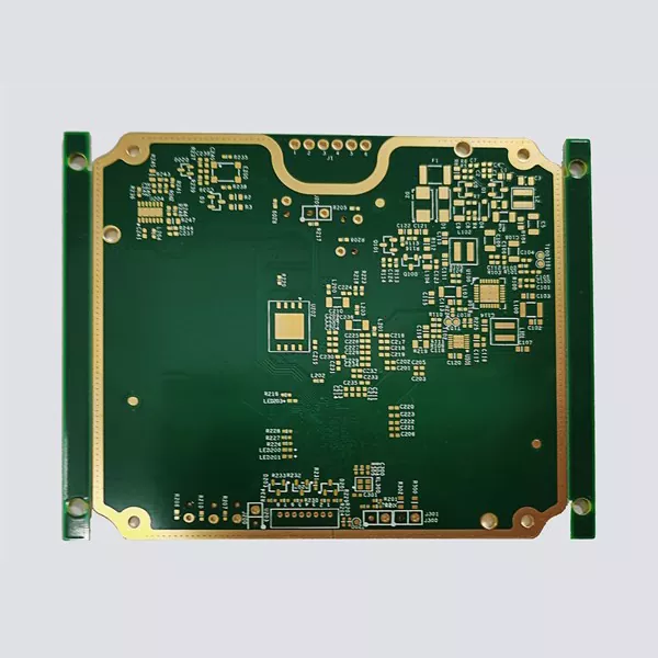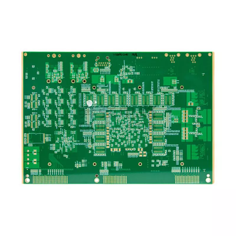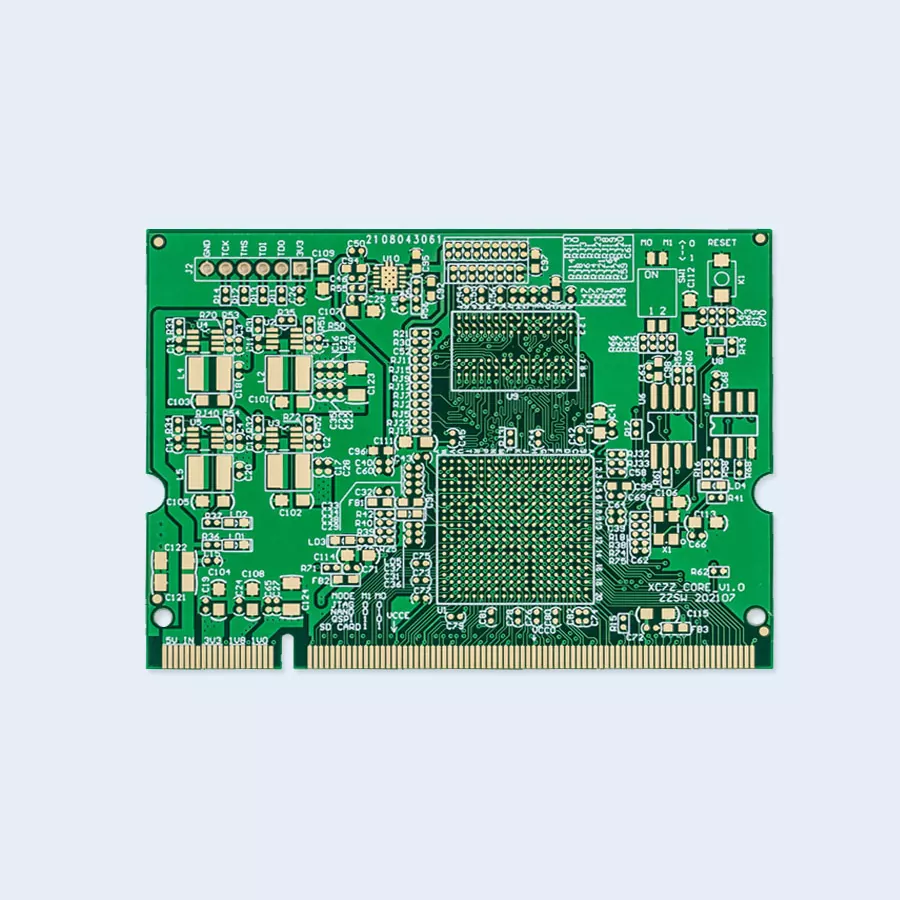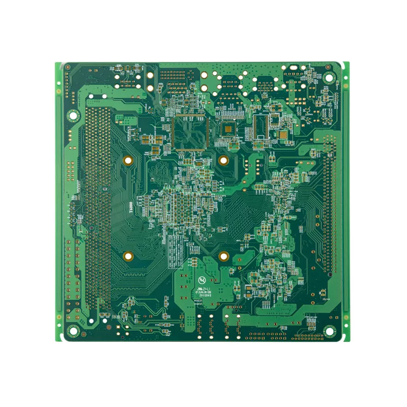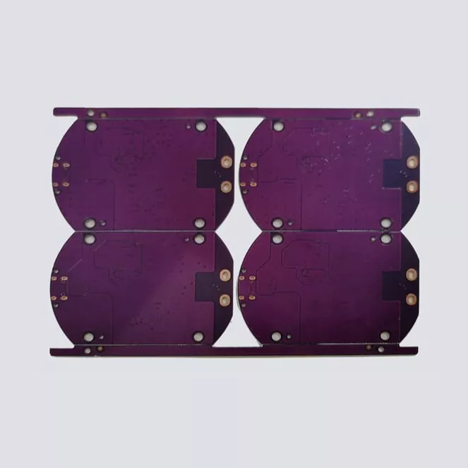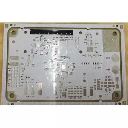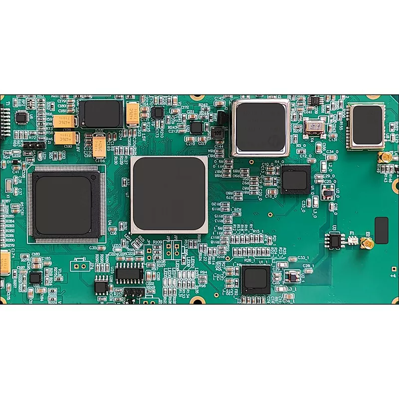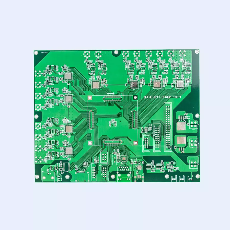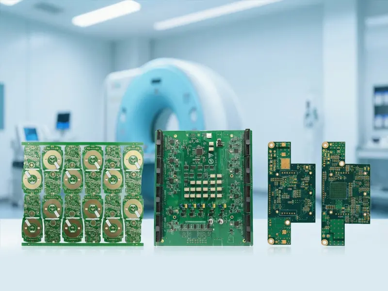

Aisen Electronics provides customized Communication Routers PCB Board solutions for Wi-Fi routers, industrial gateways, enterprise networking equipment, and advanced communication terminals. By combining multilayer PCB structures, controlled impedance technology, precision manufacturing, and PCB assembly capabilities, Aisen helps communication equipment manufacturers achieve stable signal transmission, efficient data processing, and dependable long-term operation.
A modern router is no longer a simple device for connecting computers to the internet. Today's networking equipment integrates high-performance processors, memory, wireless modules, Ethernet interfaces, power management circuits, and increasingly complex communication technologies into compact enclosures. The PCB connecting these systems directly influences signal integrity, thermal performance, electromagnetic compatibility, and overall product reliability.
A well-designed Communication Routers PCB Board therefore needs more than basic electrical connectivity. It must support high-speed transmission, high component density, controlled impedance, effective heat dissipation, and stable operation under continuous workloads. This article explains the key design requirements, manufacturing capabilities, application areas, surface finishes, quality considerations, and assembly services that buyers should evaluate when sourcing router PCB solutions.
Table of Contents
- Why Is a Communication Routers PCB Board So Important?
- What Are the Main PCB Design Requirements?
- How Does the PCB Support High-Speed Data Transmission?
- Why Are Multilayer and HDI Structures Important?
- What PCB Capabilities Should Buyers Consider?
- What Router Applications Can Use These PCB Solutions?
- How Does Thermal Management Affect Router PCB Reliability?
- How Is a Communication Router PCB Manufactured?
- Which Surface Finish Is Suitable for Router PCBs?
- Why Consider PCB Assembly Services?
- How Is PCB Quality Controlled?
- Frequently Asked Questions
- Conclusion
Why Is a Communication Routers PCB Board So Important?
The PCB is effectively the electrical backbone of a communication router. It connects the processor, memory, wireless chipset, Ethernet ports, power circuits, and other functional modules while controlling how electrical signals travel through the system.
As networking speeds increase, PCB performance becomes increasingly important. A poorly designed board may create signal distortion, electromagnetic interference, thermal problems, or unstable connections. These issues can ultimately affect network throughput and product reliability.
A professional router PCB manufacturer must therefore consider both electrical and mechanical requirements during the development stage. Important factors include:
- High-speed signal integrity
- Controlled impedance
- Multilayer stackup design
- Compact component placement
- Thermal management
- EMI and electromagnetic compatibility
- Power distribution stability
- Long-term manufacturing consistency
What Are the Main PCB Design Requirements?
Communication routers combine multiple high-speed interfaces and electronic functions in a relatively small physical space. PCB design must therefore balance electrical performance, component density, thermal requirements, manufacturability, and cost.
One of the most important considerations is the PCB stackup. Multilayer construction provides dedicated routing, power, and ground layers, helping engineers organize complex circuits while maintaining controlled electrical characteristics.
Designers also need to carefully control trace width, spacing, via structures, reference planes, and component placement. For high-frequency signals, even relatively small variations can influence transmission performance.
Aisen Electronics focuses on optimized stackup design, precision routing, and manufacturing control to support router PCB applications that demand consistent electrical performance.
How Does the PCB Support High-Speed Data Transmission?
High-speed networking requires the PCB to preserve signal quality as data moves between processors, memory devices, Ethernet interfaces, wireless modules, and other components.
Controlled impedance is particularly important for high-frequency communication circuits. By designing PCB traces and dielectric structures according to the target electrical characteristics, manufacturers can help reduce signal reflections and transmission distortion.
Other important techniques include:
- Controlled impedance routing: Helps maintain predictable electrical performance for high-speed signals.
- Optimized layer stackup: Provides appropriate signal, power, and ground structures.
- Fine-line technology: Supports compact and complex routing layouts.
- EMI control: Helps reduce unwanted electromagnetic interference.
- Precision drilling: Supports reliable electrical connections between PCB layers.
These design considerations become especially important for enterprise routers, wireless communication equipment, industrial gateways, and other devices expected to handle continuous network traffic.
Why Are Multilayer and HDI Structures Important?
Modern routers continue to add more functions without significantly increasing enclosure size. This creates a demand for higher PCB circuit density.
Multilayer PCBs provide additional routing space by stacking multiple conductive layers inside a single board. HDI technology can further improve component integration through microvias and finer circuit structures.
For compact networking equipment, these technologies can provide several advantages:
- More routing capacity within limited board dimensions
- Improved component integration
- Shorter interconnection paths
- Better support for fine-pitch components
- Greater flexibility for advanced communication designs
According to Aisen's published capabilities, its PCB manufacturing range supports 1–32 layers, minimum 3/3 mil line width and spacing, PCB thickness from 0.3 mm to 5.0 mm, copper thickness up to 6 OZ, mechanical vias down to 0.2 mm, and laser microvias down to 0.1 mm. Special impedance control capability is listed at ±8%. :contentReference[oaicite:1]{index=1}
What PCB Capabilities Should Buyers Consider?
When choosing a China PCB manufacturer or communication PCB supplier, buyers should evaluate whether the supplier's manufacturing capabilities match the technical requirements of the router design.
| PCB Parameter | Aisen Capability | Why It Matters for Routers |
|---|---|---|
| Layer Count | 1–32 Layers | Supports simple to highly complex circuit structures |
| Minimum Line Width/Spacing | 3/3 mil | Supports high-density routing |
| PCB Thickness | 0.3–5.0 mm | Provides flexibility for different product structures |
| Copper Thickness | Up to 6 OZ | Supports different current-carrying requirements |
| Minimum Mechanical Via | 0.2 mm | Supports compact multilayer interconnections |
| Laser Micro Via | Down to 0.1 mm | Supports advanced HDI PCB structures |
| Special Impedance Control | ±8% | Helps maintain high-speed signal performance |
| HDI Structure | 1+N+1 / 2+N+2 | Supports compact, high-density communication products |
Actual production specifications should always be confirmed against the specific PCB design, material selection, stackup, quantity, and manufacturing requirements.
What Router Applications Can Use These PCB Solutions?
Communication router PCB technology can be adapted to different networking products according to their processing performance, interface configuration, physical size, and operating environment.
Consumer Wi-Fi Routers
Home and consumer networking products prioritize compact dimensions, reliable wireless connectivity, efficient power consumption, and cost-effective manufacturing. PCB layouts typically integrate wireless chipsets, processors, memory, Ethernet interfaces, antenna connections, and power circuits.
Industrial Routers and Gateways
Industrial networking equipment often operates continuously and may face more demanding environmental conditions. PCB solutions need to emphasize durability, stable power distribution, thermal performance, and long-term operational reliability.
Enterprise Communication Routers
Enterprise routers generally require greater processing capability and multiple high-speed communication interfaces. Their PCBs may contain complex multilayer routing and higher component densities to support continuous data exchange.
Wireless Communication Equipment
Wireless communication products place additional emphasis on RF-related layout considerations, signal integrity, antenna connectivity, and electromagnetic compatibility.
How Does Thermal Management Affect Router PCB Reliability?
Routers frequently operate for long periods without interruption. Processors, wireless modules, power management components, and other active devices generate heat during operation.
If heat is not effectively managed, excessive temperature can influence component reliability and system stability. PCB design can therefore contribute to thermal performance through copper distribution, component placement, thermal vias, and appropriate heat dissipation structures.
A well-planned board should consider thermal performance from the beginning rather than treating it as a final-stage correction. For demanding communication equipment, electrical performance and thermal management should be evaluated together.
How Is a Communication Router PCB Manufactured?
Producing a reliable Communication Routers PCB Board requires precise process control from material preparation through final electrical testing.
- Material inspection: Incoming materials are checked according to project specifications.
- Inner-layer processing: Circuit patterns are transferred and processed with controlled accuracy.
- Layer lamination: Multilayer structures are assembled under controlled process conditions.
- Precision drilling: Mechanical and specialized drilling processes create interlayer connections.
- Copper plating: Conductive connections are established through the required PCB layers.
- Circuit formation: External circuitry is formed according to the approved design.
- Surface treatment: The selected surface finish is applied according to assembly requirements.
- AOI inspection: Automated optical inspection helps identify manufacturing defects.
- Electrical testing: Electrical continuity and isolation are evaluated before shipment.
- Final verification: Finished boards are checked against customer specifications.
For complex multilayer communication boards, additional inspection can help verify layer alignment, circuit accuracy, and interconnection reliability.
Which Surface Finish Is Suitable for Router PCBs?
Surface finish selection should be based on component type, assembly technology, expected reliability, and cost requirements.
| Surface Finish | Typical Advantage | Potential Application |
|---|---|---|
| ENIG | Suitable for fine-pitch components and high-reliability applications | Advanced communication equipment |
| OSP | Cost-effective surface protection | Standard router PCB applications |
| HASL / Lead-Free HASL | Reliable conventional assembly option | General electronic products |
| Immersion Silver / Tin | Suitable for specific performance requirements | Selected communication electronics |
The appropriate finish should be determined according to the PCB design and assembly process rather than selected solely according to price.
Why Consider PCB Assembly Services?
For router manufacturers, purchasing bare PCBs and managing component assembly through separate suppliers can increase coordination requirements. An integrated PCB and PCBA supplier can simplify procurement and production management.
Aisen Electronics provides PCB assembly support including:
- Component sourcing
- SMT assembly
- Precision component placement
- Inspection and quality verification
- Electrical testing
- Production support for communication equipment
This approach allows networking equipment manufacturers to coordinate PCB fabrication and assembly through a single manufacturing partner, potentially improving production efficiency and simplifying supplier management.
How Is PCB Quality Controlled?
Quality consistency is critical for communication equipment because a PCB defect can affect network stability, product availability, and customer experience.
A robust quality management process should cover the complete manufacturing chain rather than relying only on final inspection. Key checkpoints include incoming material inspection, production monitoring, AOI inspection, electrical testing, and final verification.
For buyers evaluating a Communication Routers PCB Board manufacturer, it is useful to review not only equipment capabilities but also inspection procedures, engineering communication, prototype support, production consistency, and the supplier's ability to follow customer specifications.
Frequently Asked Questions
What is a Communication Routers PCB Board?
A Communication Routers PCB Board is the main circuit board used inside communication routers to connect processors, memory, wireless modules, network interfaces, power circuits, and other electronic components required for data communication.
Why does a router PCB need impedance control?
High-speed router signals are sensitive to impedance variations. Proper impedance control can help reduce signal reflection and distortion, supporting more stable high-speed communication performance.
Can a communication router PCB be manufactured with multiple layers?
Yes. Multilayer construction is commonly used for advanced router applications because it provides additional routing capacity and allows signal, power, and ground structures to be organized more effectively. Aisen's published capability covers PCB designs from 1 to 32 layers.
Can router PCB manufacturers provide PCBA services?
Yes. Integrated PCB assembly services can include component sourcing, SMT placement, inspection, and electrical testing. This can help networking equipment manufacturers simplify their supply chain.
What types of routers can use customized router PCBs?
Customized router PCB solutions can be developed for consumer Wi-Fi routers, enterprise routers, industrial routers, wireless networking products, gateways, and other communication terminals, depending on the required electrical and mechanical specifications.
What information is required for a PCB quotation?
For an accurate quotation, buyers should normally provide Gerber files, BOM files, PCB dimensions, layer count, material requirements, surface finish, expected quantity, assembly requirements, and application information.
Conclusion
A high-performance router depends on more than powerful processors and advanced communication chips. The PCB underneath these components determines how effectively the electronic system can transmit signals, distribute power, manage heat, and maintain reliable connections. For this reason, choosing the right Communication Routers PCB Board manufacturing partner is an important part of developing dependable networking equipment.
With multilayer PCB manufacturing, HDI capabilities, controlled impedance technology, precision fabrication, PCB assembly, inspection, and customized engineering support, Aisen Electronics can provide solutions for a wide range of communication networking applications. If you are sourcing a reliable China PCB manufacturer or developing a new router, gateway, or wireless communication product, contact us to discuss your PCB requirements, technical specifications, prototype needs, and volume production plans.