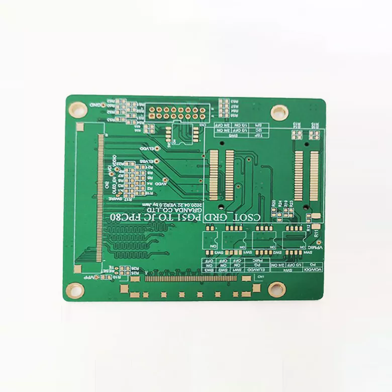
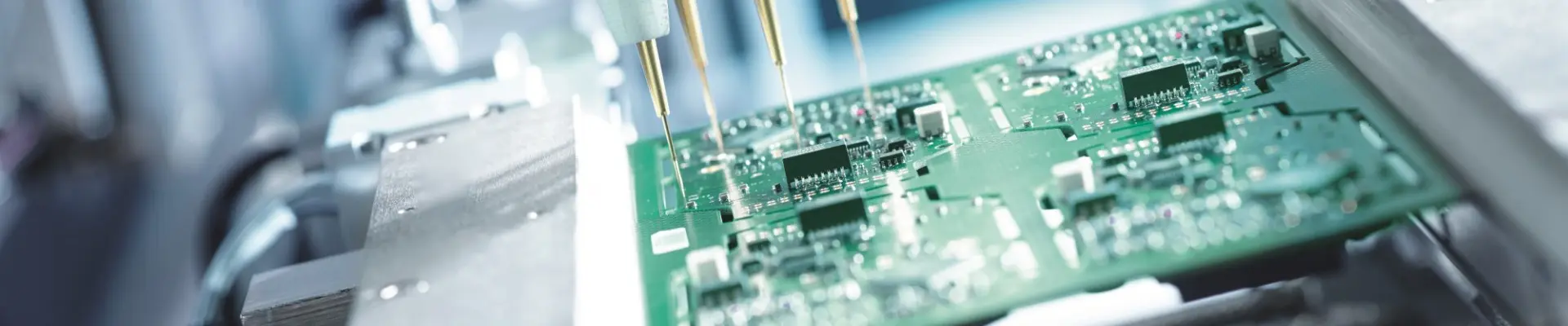
Customized Communications PCB and PCBA manufacturing solutions
Modern communication systems rely on printed circuit boards to maintain stable signal transmission between antennas, RF modules, processors, power management units, and high-speed interfaces. As communication equipment continues to move toward higher frequency bands, faster data rates, and more compact designs, PCB manufacturing accuracy becomes a critical factor affecting system performance.
Shenzhen Aisen Electronics Co., Ltd. provides Communications PCB and PCBA solutions for 5G infrastructure, wireless communication equipment, optical communication modules, network devices, and IoT terminals. With manufacturing capabilities covering 1-40 layer rigid PCB, HDI PCB, rigid-flex PCB, and PCBA assembly, Aisen Electronics focuses on controlling key parameters such as impedance consistency, dielectric performance, copper thickness uniformity, and microvia reliability.
Our communication circuit boards are manufactured in a 50,000-square-meter production facility equipped with advanced drilling, laser via, electroplating, LDI exposure, AOI inspection, and automated testing equipment. The production system supports high-density interconnection designs and complex multilayer structures required by next-generation communication products.
PCB Technologies Behind Reliable Communication Equipment
Communication PCB manufacturing is different from conventional electronic boards because signal integrity directly affects transmission quality. A minor variation in line width, dielectric thickness, or copper surface roughness may cause signal loss, impedance deviation, or electromagnetic interference problems.
For high-speed communication applications, Aisen Electronics controls PCB fabrication from material selection to final inspection. High-frequency laminates, low-loss materials, controlled impedance routing, and precise layer alignment are applied according to product requirements.
For example, communication boards used in 5G base stations often require multilayer structures with strict impedance control, while optical communication equipment requires extremely stable electrical performance for high-speed signal conversion. HDI technology is used when designers need smaller form factors with higher wiring density.
Communication PCB Types We Manufacture
5G Base Station PCB
5G infrastructure places higher requirements on PCB performance because base stations operate with high-frequency signals and massive data transmission loads.
Aisen Electronics manufactures multilayer communication boards for 5G base station units, including RF boards, power distribution boards, antenna control modules, and signal processing boards.
These PCBs typically use high-frequency and high-speed materials with controlled dielectric characteristics. During manufacturing, key processes such as lamination control, laser drilling, copper plating, and impedance testing are optimized to maintain signal consistency across complex multilayer structures.
Typical capabilities:
- • Layer count: up to 40 layers
- • Min line width/spacing: 2/2mil
- • High-frequency material compatibility
- • Controlled impedance manufacturing
- • Low-loss signal transmission
Optical Communication PCB
Optical communication equipment requires PCB solutions that support high-speed electrical signal conversion between optical modules, processors, and network systems.
Unlike ordinary communication boards, optical communication PCBs need extremely accurate circuit patterns because high-speed signals are sensitive to transmission loss and electromagnetic interference.
Aisen Electronics produces optical communication PCBs for applications such as optical transceivers, data transmission modules, and network equipment.
Manufacturing focus:
- • Stable dielectric thickness
- • Fine circuit fabrication
- • High-density interconnection
- • Reliable microvia structures
- • Surface treatment for HF
Network Equipment PCB
Routers, switches, servers, and data communication equipment require PCBs capable of handling continuous high-speed data processing.
Aisen Electronics manufactures network equipment PCBs using multilayer structures designed for high-speed digital signals. These boards often integrate high-density components, BGA packages, and complex power distribution networks.
The combination of PCB fabrication and PCBA assembly allows customers to reduce supplier coordination and improve product consistency.
Process support:
- • 8-20 layer multilayer production
- • BGA and fine-pitch assembly
- • High-density routing
- • Automated optical inspection
- • Electrical performance testing
IoT Communication PCB
IoT devices require smaller PCB sizes while integrating wireless communication modules, sensors, processors, and power management circuits.
Aisen Electronics provides compact PCB solutions for smart terminals, wireless sensors, gateway devices, and intelligent control systems.
Rigid-flex technology is especially suitable for wearable communication devices and compact electronic products where installation space is limited.
Solutions provided:
- • Miniaturized multilayer designs
- • HDI microvia structures
- • Flexible and rigid-flex options
- • SMT assembly services
- • Low-power circuit optimization
Manufacturing Capability for Communication PCB and PCBA
Aisen Electronics has developed complete PCB and PCBA production capabilities covering prototype development, engineering verification, and mass production.
| Manufacturing Item | Capability |
|---|---|
| PCB Layer Count | 1-40 layers |
| PCB Type | Rigid PCB, HDI PCB, Rigid-flex PCB, FPC |
| Maximum PCB Size | 730mm × 630mm |
| Finished Thickness | 0.3mm-5.0mm |
| Minimum Mechanical Drill | 0.15mm |
| Laser Microvia | 75μm-150μm |
| Minimum Line Width/Spacing | 0.05mm/0.05mm |
| Maximum Copper Thickness | 10oz |
| PCBA Component Size | 01005 chip capability |
| BGA Minimum Diameter | 0.22mm special capability |
Advanced Process Control for Communication Applications
Communication PCB quality depends heavily on manufacturing consistency. Aisen Electronics applies process monitoring throughout drilling, plating, imaging, solder mask, assembly, and inspection.
Impedance Control
The production team controls line width, dielectric thickness, copper thickness, and material parameters to maintain stable impedance performance.
Microvia Reliability
HDI communication boards rely on laser-drilled microvias. Aisen Electronics uses advanced laser drilling and electroplating processes to improve via reliability during thermal cycling and long-term operation.
Signal Integrity Protection
Surface copper uniformity, etching accuracy, and layer alignment are controlled to reduce signal attenuation and improve high-speed transmission performance.
Communication PCBA Assembly Services
Besides PCB manufacturing, Aisen Electronics provides PCBA assembly services for communication products. The production line supports SMT, DIP, component mounting, solder paste inspection, AOI inspection, X-ray inspection, and electrical testing.
Communication PCBA applications:
- Wireless communication modules
- Network control units
- Data transmission equipment
- IoT gateways
- Industrial communication terminals
Assembly capability:
- Fine-pitch component support
- BGA package assembly
- Compact device assembly
- Automated inspection
- Functional testing
Quality Control for Communication PCB Production
Communication equipment often operates continuously in demanding environments, making PCB reliability essential. Aisen Electronics implements ISO9001, ISO14001, and IATF16949 quality management systems.
Inspection equipment:
- AOI automatic optical inspection
- AVI visual inspection
- X-ray inspection
- Impedance testing
- High-current testing
- Metallographic analysis
- Hole inspection
- Copper thickness measurement
Quality targets:
- Product yield ≥99.8%
- On-time delivery rate ≥99%
- Customer complaint rate ≤0.5%
Why Choose Aisen Electronics for Communications PCB and PCBA
With more than 20 years of PCB manufacturing experience, Shenzhen Aisen Electronics Co., Ltd. provides integrated PCB and PCBA manufacturing services for global communication equipment companies.
High-Layer Capability
Up to 40 layers for complex designs
HDI & Rigid-Flex
High-density and flexible solutions
Integrated PCBA
PCB + SMT + testing services
Supported by advanced production equipment, experienced engineering teams, and mature supply chain management, Aisen Electronics helps communication manufacturers shorten development cycles and improve product reliability from prototype to mass production.
FAQ
What type of PCB is commonly used in communication equipment?
Communication equipment usually uses multilayer PCB, HDI PCB, and high-frequency PCB because these structures provide higher wiring density and better signal transmission performance.
Can Aisen manufacture high-frequency communication PCB?
Yes. Aisen Electronics supports high-frequency and high-speed PCB manufacturing with controlled impedance processes and suitable material solutions.
What layer count can your communication PCB support?
Aisen Electronics manufactures communication PCBs from 1 to 40 layers according to customer design requirements.
Do you provide communication PCBA assembly?
Yes. Aisen Electronics provides PCB manufacturing combined with SMT and DIP assembly services.
What inspection methods are used for quality control?
Inspection includes AOI, AVI, X-ray inspection, impedance testing, copper thickness measurement, and electrical testing.
Can you manufacture HDI PCB for 5G applications?
Yes. HDI PCB manufacturing is one of Aisen Electronics' core capabilities and is suitable for compact 5G communication equipment.
- View as
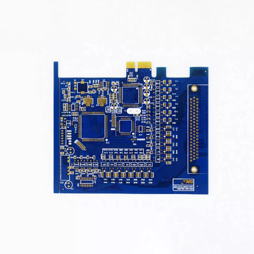
Communication Data Centers PCB
**Communication Data Centers PCB Summary(约300字符):**
Shenzhen Aisen Electronics Co., Ltd. provides Communication Data Centers PCB solutions for high-speed networking, server systems, and power management equipment. Designed with multilayer structures, HDI technology, controlled impedance, and high-current capability, these PCBs ensure stable signal transmission, efficient heat management, and long-term reliability in 24/7 data center operations. We support prototype to mass production with strict testing and process control.
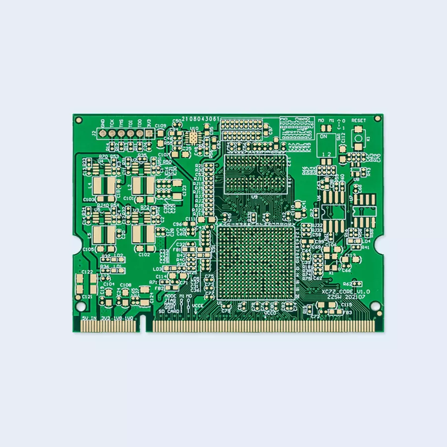
PCB Assembly for Communication Network Devices
Aisen Electronics Co., Ltd. provides PCB assembly for communication network devices. Our manufacturing capabilities support high-speed signal transmission, high-density component integration, thermal management, and reliable 24/7 operation in modern communication systems.
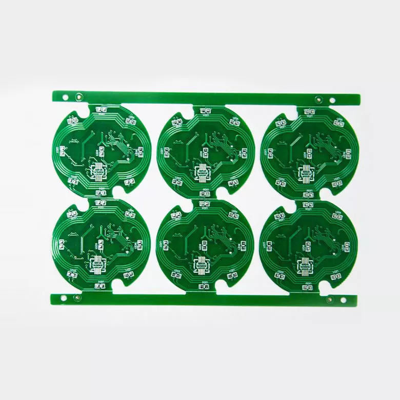
Communication Switches PCB Board
When your project demands exceptional reliability and precision, our communication switches pcb board fabricating administrations convey the quality you require. We specialize in making high-performance sheets that control today's progressed communication foundation. Whether you're creating organize gear, IoT gadgets, or complex communication frameworks, our ability guarantees your communication switches meets the most noteworthy industry standards.
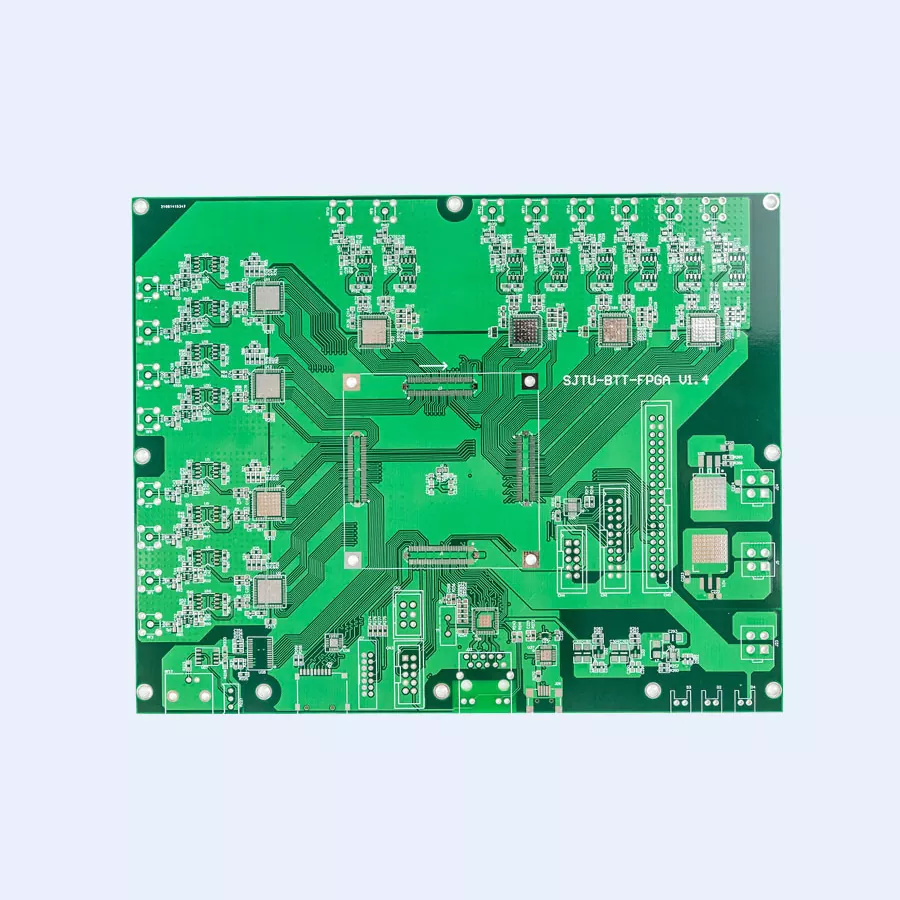
Communication Routers PCB Board
Aisen Electronics Co., Ltd. provides customized PCB board manufacturing solutions for communication routers, wireless routers, industrial gateways, and network control equipment. Our Communication Routers PCB Board are designed to support high-speed data processing, stable signal transmission, and reliable operation in modern communication environments.
From compact home networking products to industrial-grade communication systems, we provide PCB solutions optimized for processor integration, wireless modules, power management, and long-term network performance.
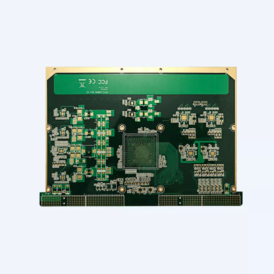
Communication Servers PCB
When your communication framework requests unwavering quality and execution, you require a communication servers pcb producer that gets it the basic nature of organize gear. At Shenzhen Aisen Electronics Co., Ltd., we specialize in conveying high-quality printed circuit sheets planned particularly for communication servers and organizing applications. Our progressed fabricating forms guarantee your communication servers meets the rigid prerequisites of present day information centers and broadcast communications infrastructure.
As a reliable Communications PCB and PCBA manufacturer and supplier in China, we have our own factory. We provide high-quality PCB manufacturing services with customized solutions for global electronic industries.