
What Makes Consumer Electronics PCB and PCBA Essential for High-Performance Electronic Products?
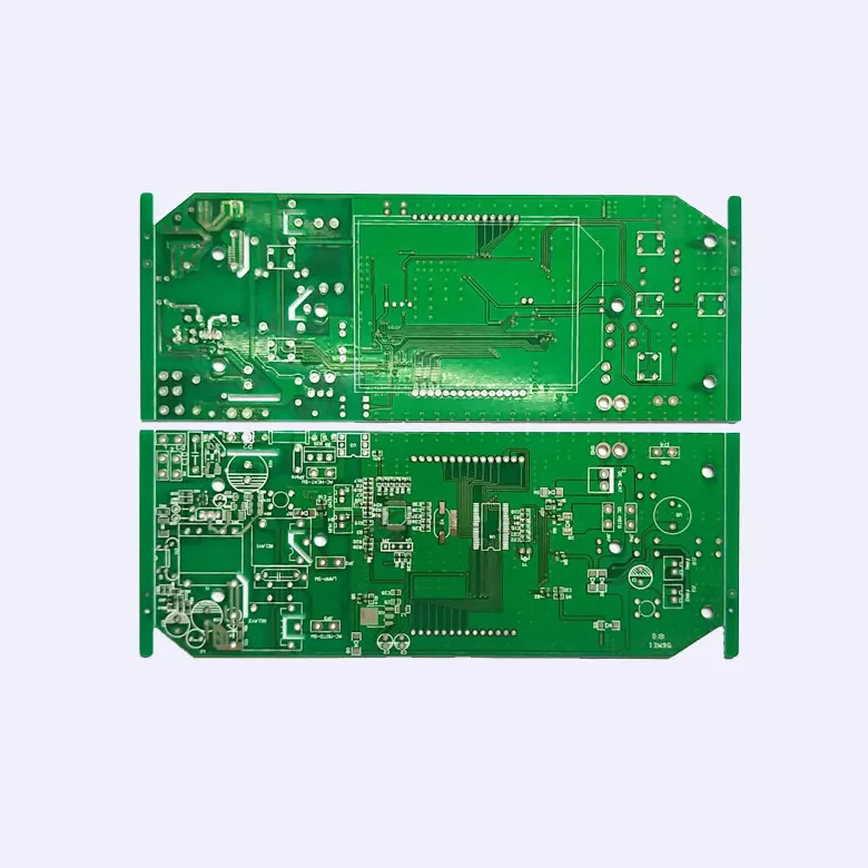
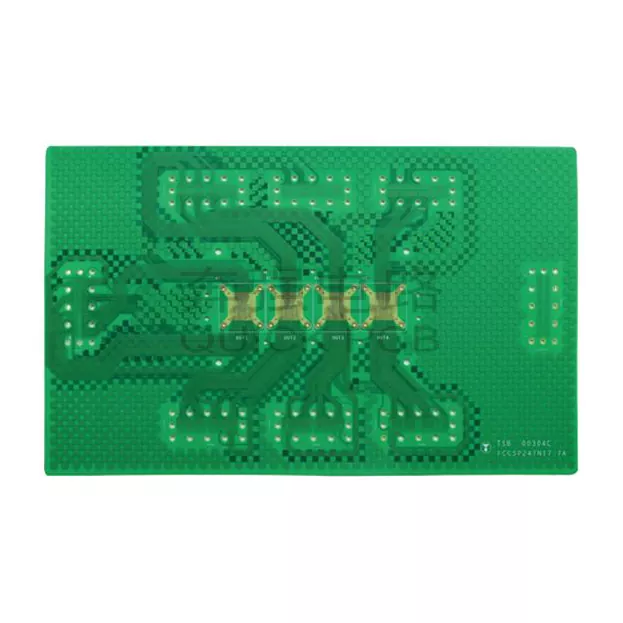
From the smartphone in your pocket to the smart speaker in your living room, the seamless functionality and high performance of modern consumer electronics are powered by two unsung heroes: the Printed Circuit Board (PCB) and the Printed Circuit Board Assembly (PCBA). A Consumer Electronics PCB and PCBA are the structural and electrical backbone of any device, providing the critical interconnectivity that allows components to communicate and function as a unified system. Without a meticulously designed, reliably manufactured PCB and a flawlessly executed assembly process, the most advanced processors and cutting-edge sensors would be nothing more than a collection of disconnected silicon pieces. The relentless consumer demand for smaller, faster, more powerful, and feature-rich devices has placed immense pressure on the PCB and PCBA industry. At Shenzhen Aisen Electronics Co.,Ltd., our factory has been at the forefront of this evolution, adapting our processes to meet the stringent requirements of 5G, artificial intelligence, and IoT applications. This article will explore the multi-faceted reasons why PCB and PCBA are not just components, but the essential enablers of high-performance electronic products.
The journey from a conceptual electronic design to a tangible, high-performance product is a complex one, and the PCB and PCBA are the physical manifestation of that design. A high-performance product requires a high-performance foundation. This foundation is built upon three critical pillars: the ability to manage high-speed signal integrity to prevent data loss and interference, the capacity to efficiently dissipate heat to ensure device longevity and reliability, and the capability to accommodate increasingly miniaturized components without sacrificing performance. Furthermore, in the consumer electronics space, where margins are tight and time-to-market is critical, the reliability and consistency of the PCB and PCBA supply chain are paramount. A single production defect can lead to a wave of returns, damaging brand reputation and profitability. As we delve deeper into the technical and operational aspects of PCB and PCBA, we will uncover the specific design rules, manufacturing techniques, and rigorous testing protocols that differentiate a merely functional board from one that truly enables high performance and long-term reliability.
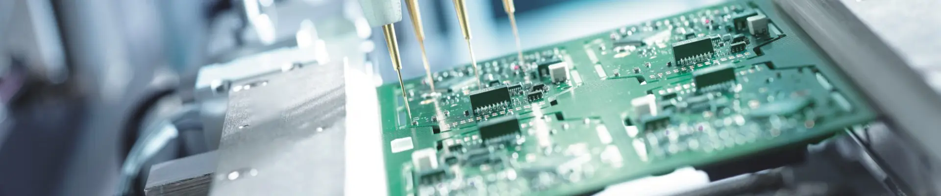
Table of Contents
- 1. What is the Evolution of Consumer Electronics PCB?
- 2. How Does PCBA Solve the Challenges of Miniaturization?
- 3. What Technical Specifications Define High-Performance PCB?
- 4. How Do Advanced Manufacturing Processes Enhance Reliability?
- Frequently Asked Questions (FAQ)
- Conclusion and Project Consultation
What is the Evolution of Consumer Electronics PCB?
To understand why Consumer Electronics PCB and PCBA are essential for high-performance products today, it is instructive to look at their evolution. The journey from the bulky, single-sided PCBs of the 1960s to the incredibly dense, multi-layer, and flexible circuits we use now is a testament to the relentless pursuit of miniaturization and performance. In the early days, a PCB's primary function was to replace point-to-point wiring, making electronic devices more reliable and easier to manufacture. As the integrated circuit (IC) emerged and began to grow in complexity, the role of the PCB expanded from a simple wiring substrate to a carefully engineered interconnect that had to manage electrical signals with ever-increasing frequencies and speeds.
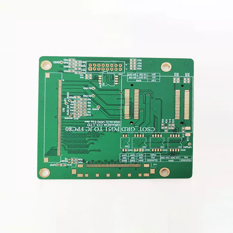
Consider the example of the mobile phone. The first generation of mobile phones in the 1980s used 1-2 layer PCBs with relatively generous trace widths and spacing. The Nokia 3310 from 2000 used a compact multi-layer board, but still with a relatively simple signal architecture. Fast forward to today’s 5G smartphones. They use high-density interconnect (HDI) boards with up to 12 layers, embedded components, and microvias that are virtually invisible to the naked eye. This evolutionary leap was not driven by a desire for complexity for its own sake; it was a direct response to the need for faster processing power, higher bandwidth, and multiple functionality in a shrinking form factor. The PCB had to evolve to handle the noise from these high-speed signals while maintaining signal integrity, all within a device that could fit in the palm of your hand.
This evolutionary process has fundamentally changed the role of the PCB manufacturer. It is no longer a job of simply routing traces according to a netlist. It has transformed into a highly collaborative engineering discipline. A manufacturer must now work closely with the system designer from the very beginning, providing design for manufacturability (DFM) feedback on material selection, stack-up design, and routing constraints. For instance, a high-speed interface like USB 3.1 or PCIe will require a very specific impedance control. Our factory at Aisen has invested heavily in the technology needed to support this evolution. Our technical team uses advanced simulation tools to model the performance of the PCB before it is ever manufactured, ensuring that the design is optimized for signal integrity and manufacturability. We have also expanded our capabilities to meet the demands of high-performance devices, such as the ability to manufacture complex HDI boards with laser-drilled microvias, and the expertise to process advanced materials like Rogers or Isola for high-frequency applications. This deep technical engagement is what enables us to deliver Consumer Electronics PCB and PCBA solutions that truly unlock the performance potential of next-generation electronic products.
How Does PCBA Solve the Challenges of Miniaturization?
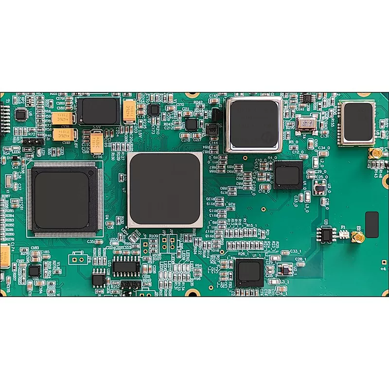
Miniaturization is the defining trend in the consumer electronics industry. Consumers want more processing power, longer battery life, and more sensors, all in a device that is thinner, lighter, and more aesthetically pleasing. This relentless drive toward miniaturization places enormous challenges on the assembly process, which is where the PCBA (Printed Circuit Board Assembly) phase becomes critical. It is not enough to design a dense, intricate PCB; the components must be placed and soldered onto that board with extreme precision and reliability. A poorly executed assembly can completely undermine the design of the most sophisticated PCB, leading to electrical shorts, open connections, or failure due to poor thermal performance.
One of the most significant challenges in miniaturization is component placement. Components have shrunk to the point where they can barely be seen by the naked eye; for example, the common 0201 resistor (0.6mm x 0.3mm) and the even more challenging 01005 (0.4mm x 0.2mm) are now common in compact consumer products. Placing these components manually is impossible, and even with automated equipment, the demands on placement accuracy are incredibly stringent. Our factory uses the latest generation of high-speed pick-and-place machines that can place components with an accuracy of +/- 25 microns. This is achieved through a combination of high-resolution cameras and sophisticated software that performs optical alignment checks before, during, and after placement. This process is further enhanced by a rigorous stencil printing process for applying solder paste. The paste is applied through a laser-cut stencil with apertures designed to match the pad size and shape of these ultra-small components, ensuring just the right amount of solder paste is deposited to create a reliable joint without causing shorts.
Another crucial element in the assembly of high-performance consumer electronics is the reflow soldering process. The solder joints must be of the highest quality, free from voids and defects that could lead to early failure. We have implemented a closed-loop reflow oven control system that monitors the temperature profile of each board as it passes through the oven, adjusting the heat zones in real-time to ensure that the solder reaches the optimal melting temperature. This is especially important for boards with mixed technology, such as those containing both fine-pitch BGAs (Ball Grid Arrays) and larger, heat-sensitive connectors. Our factory uses nitrogen-assisted reflow for critical assemblies. By creating an inert atmosphere, we reduce the risk of oxidation on the solder joints, resulting in a brighter, stronger, and more reliable connection. These steps, from precision stencil printing to controlled reflow, are the practical ways we solve the challenges of miniaturization, ensuring that the Consumer Electronics PCB and PCBA we deliver are ready for the most demanding applications.
What Technical Specifications Define High-Performance PCB?
Defining a high-performance PCB goes beyond the basic dimensions of length, width, and thickness. It involves a set of critical technical parameters that are carefully engineered to ensure the board can support the demands of modern, high-speed electronic devices. These specifications are the language through which a designer communicates the requirements, and a manufacturer demonstrates its capability. The selection of materials, the layout of the layers, and the design of the interconnects are all dictated by the electrical and thermal needs of the device. For a consumer electronics product to achieve its peak performance, the PCB must be designed and manufactured to these exacting standards.
To effectively evaluate a PCB's capabilities, it is helpful to understand the key technical specifications and what they mean. The table below illustrates some of the critical parameters we routinely address in our design and manufacturing processes.
| Parameter | Typical Specification | Impact on Performance |
| Dielectric Constant (Dk) | 3.0 - 4.5 (material dependent) | Affects signal propagation speed; critical for high-frequency impedance matching. |
| Dissipation Factor (Df) | 0.001 - 0.01 | Determines signal loss; lower values are essential for high-speed, high-frequency applications. |
| Thermal Conductivity (W/m·K) | 0.3 - 1.0 (standard FR4) | Manages heat dissipation; higher values are required for high-power devices to prevent hotspots. |
| Impedance Control (Ω) | 50Ω, 75Ω, 90Ω, 100Ω | Ensures signal integrity on controlled impedance traces; prevents reflections and data errors. |
| Copper Weight (oz) | 0.5oz to 2oz (inner layers), 1oz to 3oz (outer layers) | Defines current-carrying capacity and thermal conductivity of the traces. |
| Minimum Trace Width/Spacing | 3mil/3mil (standard) or less (HDI) | Enables high-density routing; critical for miniaturization. |
| Minimum Mechanical Hole Size | 0.2mm (standard), 0.1mm (laser drilled) | Allows for component leads; smaller holes are essential for HDI and BGA packages. |
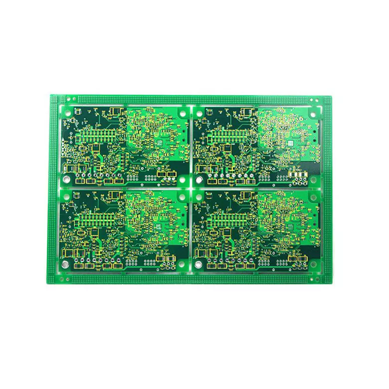
In addition to these standard parameters, high-performance PCBs often require special considerations. For example, a PCB for a 5G base station will require very low Df materials like PTFE or ceramic-filled hydrocarbon to maintain signal integrity at multi-gigahertz frequencies. A PCB for a power inverter will need heavy copper layers to handle high currents and thermal vias to channel heat away from the power components. Our factory at Shenzhen Aisen Electronics Co.,Ltd. has a broad portfolio of advanced materials and processes to support these diverse needs. We have extensive experience with a wide range of high-performance materials and can provide expert guidance on selecting the optimal material set for the specific performance requirements of your Consumer Electronics PCB and PCBA. This expertise is not just about understanding the materials; it's about understanding the complex interplay between material properties, circuit layout, and manufacturing process, ensuring the final product performs as intended.
How Do Advanced Manufacturing Processes Enhance Reliability?
The reliability of a consumer electronic product is directly tied to the reliability of its PCB and PCBA. Even the most perfect design can be undone by manufacturing defects such as solder voids, micro-cracks, or poor plating. High-performance devices demand manufacturing processes that go far beyond industry standards to ensure a level of reliability that can withstand the rigors of daily use, environmental stress, and long operating hours. This is where the investment in advanced manufacturing capabilities and a culture of quality becomes the key differentiator.
The process begins with the PCB fabrication itself. Our factory is equipped with a state-of-the-art plasma etching system for cleaning the board surface before the lamination process. This advanced method creates micro-roughening on the surface, dramatically improving the bond strength between the dielectric layers and the copper, which is critical for preventing delamination under thermal stress. We then use advanced laser drilling systems to produce microvias, which are essential for high-density interconnect (HDI) designs. These systems can achieve precise microvia diameters of 100µm and below, enabling the layer-to-layer connections required for complex, high-performance devices. This is followed by an automated optical inspection (AOI) system that uses high-resolution cameras to inspect the board for defects such as opens, shorts, and insufficient copper, ensuring the integrity of the board before assembly.
During the PCBA phase, we deploy a range of advanced inspection technologies that ensure the quality of every solder joint. For example, we use 3D automated optical inspection (AOI) machines that look at the shape of the solder joints from multiple angles to detect faults like insufficient wetting, component skew, or solder bridging. For highly critical boards, especially those with many BGA components, we use 3D X-ray inspection. This non-destructive technique allows us to look through the component and inspect the solder joints underneath, detecting voids that are invisible to standard AOI. We have established a systematic approach to continuously monitor these inspection results. This data is fed back into the process to help us optimize it, reducing variation and improving yields over time. This commitment to both advanced technology and data-driven process control ensures that the Consumer Electronics PCB and PCBA leaving our factory are not only high-performing but also remarkably reliable.
Frequently Asked Questions (FAQ)
Question 1: What type of PCB material is best for high-speed digital consumer electronics?
Answer: The choice depends on the operating frequency of the signals. For standard high-speed digital, such as DDR memory or USB 3.0, standard FR-4 is often sufficient when properly controlled. For signals in the multi-gigahertz range, such as those found in 5G or high-speed networking devices, materials like Rogers/Isola with low dielectric constant and low dissipation factor are required to maintain signal integrity. Our engineering team can help you select the right material for your specific application based on your performance and budget requirements.
Question 2: What is the difference between PCB and PCBA?
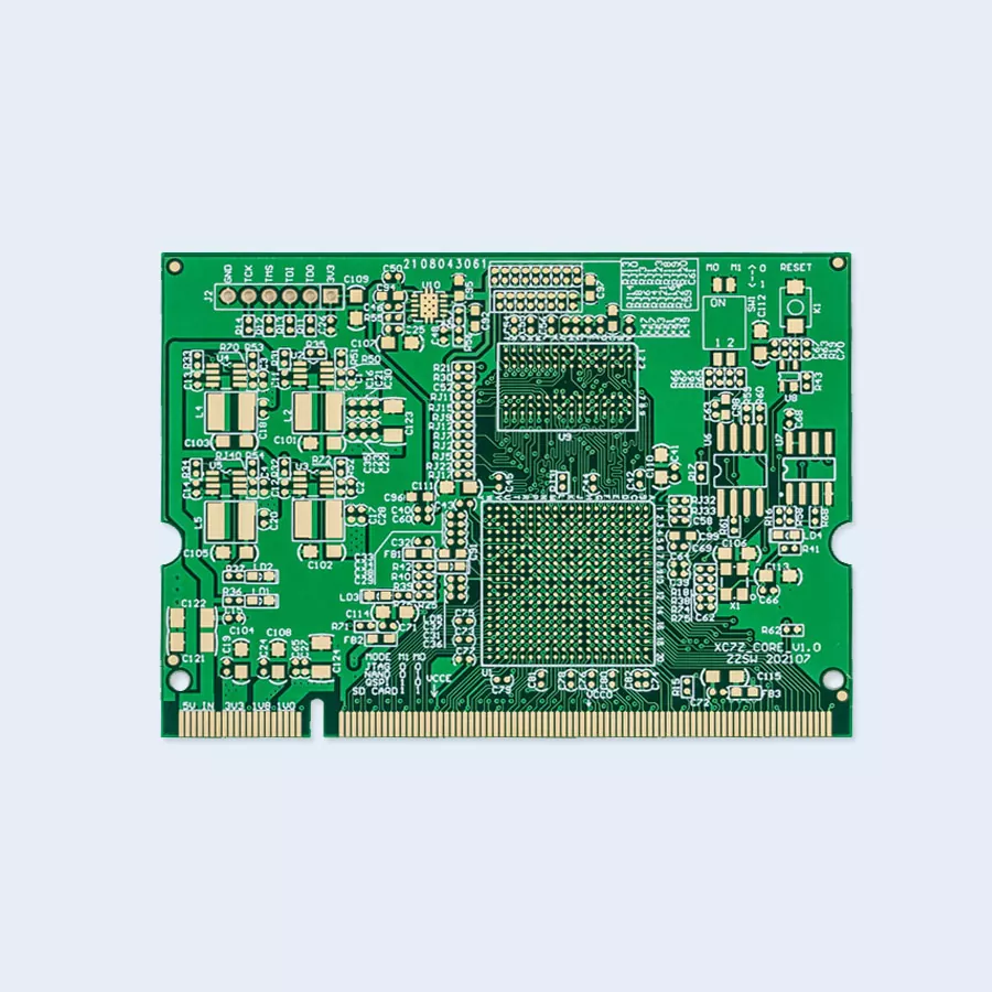
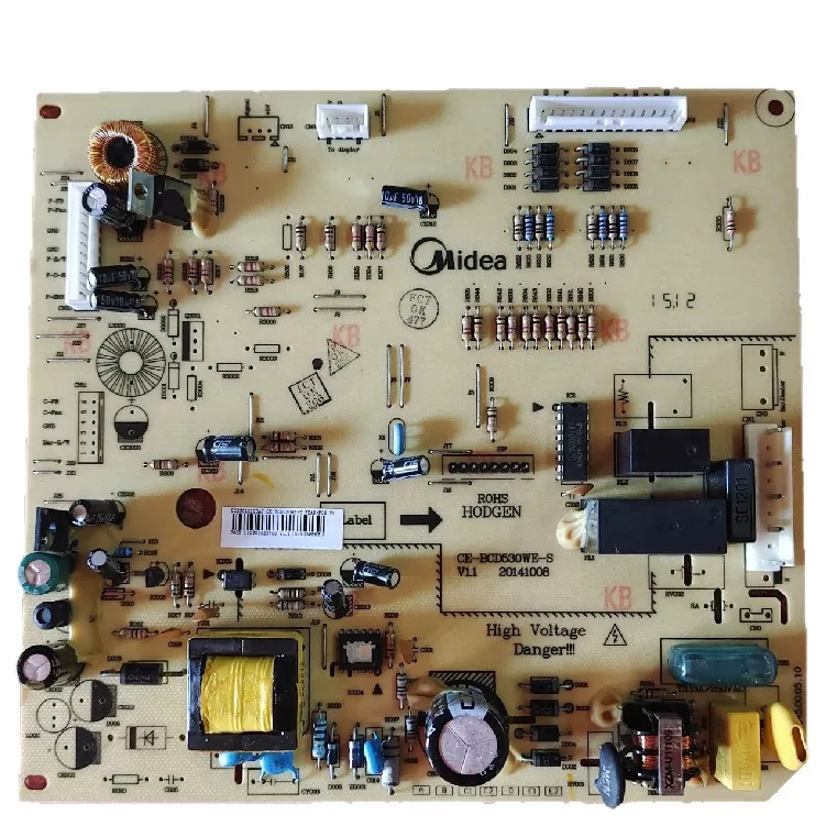
Answer: A PCB (Printed Circuit Board) is the bare board—the fiberglass substrate with copper traces and pads, but without any electronic components. A PCBA (Printed Circuit Board Assembly) is the final, functional board that has been populated with components through processes like SMT and through-hole soldering. The PCBA is what goes into your electronic device. Shenzhen Aisen Electronics Co.,Ltd. provides both services, delivering a complete manufacturing solution for Consumer Electronics PCB and PCBA.
Question 3: How does a manufacturer ensure consistent PCBA quality across large production runs?
Answer: Consistency is achieved through a combination of automated manufacturing, statistical process control, and rigorous quality management systems. This includes the use of high-precision automated assembly lines, real-time monitoring of processes like stencil printing and reflow, regular calibration of equipment, and comprehensive final inspection using AOI and X-ray. This ensures that the first board and the ten-thousandth board are built to the same exacting standard.
Question 4: Can Shenzhen Aisen Electronics Co.,Ltd. support prototypes and new product introductions (NPI)?
Answer: Yes, we provide a complete range of support from initial prototype runs to high-volume production. Our factory is set up to handle quick-turn prototypes, allowing you to test and refine your design before committing to mass production. We offer Design for Manufacturability (DFM) reviews to optimize your design for our processes, ensuring a smooth transition from prototype to production and reducing time-to-market.
Question 5: What are the typical lead times for Consumer Electronics PCB and PCBA?
Answer: Lead times are variable and depend on the complexity of the board and the quantity required. For standard prototype runs of simple boards, we can often deliver within 5-7 days. For complex, multi-layer HDI boards in high volume, the lead time is typically 3-4 weeks. We work closely with our customers to provide the most accurate lead time estimates based on their specific project parameters and are proactive in managing schedules to meet tight deadlines.
Conclusion: Partnering for High-Performance Success
The journey from a high-performance electronic concept to a market-ready product is an intricate one, and the PCB and PCBA are the critical foundations upon which that success is built. As we have explored, they are not simply commodities but complex engineering systems that require deep expertise in materials, design, and advanced manufacturing to realize their full potential. From the evolution of the technology to the challenges of miniaturization and the rigor of quality control, every aspect of the PCB and PCBA must be meticulously managed.
If you are developing a next-generation consumer electronic device, you need a manufacturing partner that understands these complexities. Contact Shenzhen Aisen Electronics Co.,Ltd. today for a comprehensive consultation. Our expert team will work alongside you to determine the optimal PCB and PCBA solution for your specific design requirements, from material selection to final assembly and testing. We are committed to being a strategic partner in your success. Request your free consultation now from Shenzhen Aisen Electronics Co.,Ltd. and discover how our high-quality PCB and PCBA solutions can power your high-performance electronic products.
Related News
- How Can a Communication Routers PCB Board Improve High-Speed Network Performance and Reliability
- Why Is a Converter and Selector PCB Critical for High-Performance Electronic Systems
- Why Engine Control Module PCB Quality Matters for Modern Vehicle Systems
- How Does a Servo Motor PCB Improve Motion Control Reliability?
- How Can Aerospace PCB and PCBA Improve the Reliability of Modern Aerospace Systems?
- Why Is Servo Motor PCB Important in Modern Automation Systems?
Leave me a message