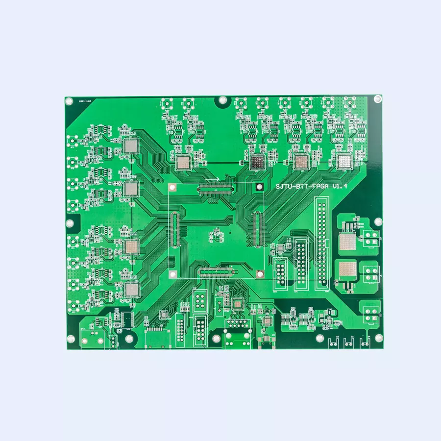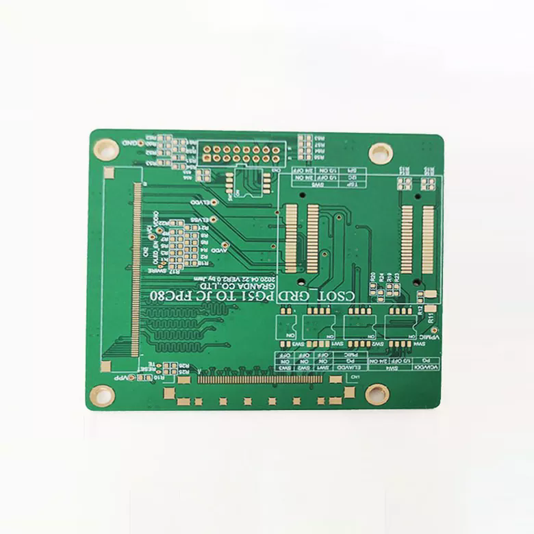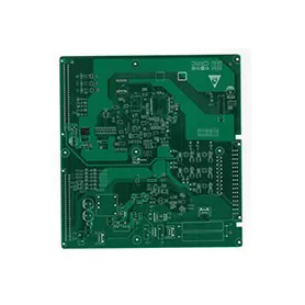
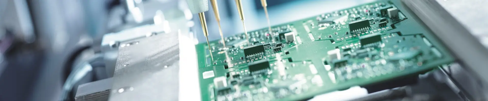
Your Reliable Semiconductor PCB and PCBA Manufacturer for Complex Electronic Solutions
Semiconductor manufacturing equipment depends on stable electronic control systems to coordinate motion modules, sensors, inspection units, power circuits, and high-speed data processing. The PCB inside these machines is required to maintain consistent electrical performance during long production cycles, where even small variations in signal transmission or connection reliability may affect equipment accuracy.
Unlike ordinary industrial control boards, Semiconductor PCB and PCBA products usually involve higher circuit density, tighter process control, and stricter reliability requirements. Boards used in wafer inspection equipment, semiconductor testing systems, and chip packaging machines often combine high-speed digital circuits, precision analog circuits, and power management functions within limited space.
Shenzhen Aisen Electronics Co., Ltd. manufactures semiconductor PCB solutions including multilayer PCB, HDI PCB, rigid-flex PCB, and PCBA assembly. With 1-40 layer PCB manufacturing capability, laser drilling technology, high-precision exposure equipment, automated inspection systems, and SMT production lines, Aisen supports semiconductor equipment manufacturers from prototype development to volume production.
Semiconductor PCB Applications in Manufacturing Equipment
Semiconductor equipment is a combination of mechanical precision, electronic control, and data processing. The PCB serves as the electrical foundation that connects different functional modules.
Test Equipment
PCB for Semiconductor Test Equipment
Automatic Test Equipment (ATE) used in semiconductor production requires PCBs capable of handling high-speed test signals, precise timing control, and stable power distribution.
Compared with standard industrial control boards, semiconductor test equipment PCB designs usually contain more signal layers and higher component density.
Typical applications:
- Chip testing systems
- IC test boards
- Burn-in test equipment
- Semiconductor measurement equipment
Inspection
PCB for Wafer Inspection Systems
Wafer inspection equipment relies on highly accurate electronic control to process optical signals, sensor feedback, and positioning data.
The PCB used in these systems needs excellent signal integrity because unstable electrical characteristics can influence measurement accuracy. High-density routing, controlled impedance, and reliable microvia structures are commonly required.
Key manufacturing considerations:
- Precise layer alignment
- Stable dielectric thickness
- Low signal interference
- Reliable microvia connection
Packaging
PCB for Semiconductor Packaging Equipment
Semiconductor packaging equipment integrates mechanical movement control, temperature management, sensors, and communication interfaces.
These machines often operate continuously in factory environments, requiring PCB assemblies with strong thermal stability and mechanical reliability.
Rigid-flex PCB technology can be used in applications where wiring space is limited or where flexible connections are required between moving modules.
Semiconductor PCB Compared With General Industrial PCB
Although both semiconductor equipment PCB and industrial control PCB are used in automation systems, their manufacturing requirements are different.
| Item | General Industrial PCB | Semiconductor PCB |
|---|---|---|
| Main function | Equipment control and power management | Precision control, testing, data processing |
| Circuit complexity | Medium density | High-density multilayer structure |
| Common PCB structure | 2-8 layers | 8-20+ layers, HDI, rigid-flex |
| Signal requirement | Standard communication | High-speed and precision signal control |
| Manufacturing focus | Basic reliability | Process consistency and electrical stability |
| Typical equipment life cycle | Several years | Long continuous operation |
For semiconductor equipment manufacturers, PCB consistency is often more important than simply achieving a low production cost.
Manufacturing Challenges of Semiconductor PCB
#1
High-Density Circuit Manufacturing
Semiconductor equipment continues to integrate more functions into smaller control units. Traditional PCB structures may not provide enough routing space for complex circuits.
Aisen capability:
- Min line/space: 0.05mm/0.05mm
- Laser drill: 75μm-150μm
- High-layer-count structures
- Fine-pitch component assembly
#2
Signal Integrity & Impedance Control
Many semiconductor systems include high-speed processors, communication modules, and precision measurement circuits. Changes in copper thickness, dielectric thickness, or line width may influence impedance performance.
Aisen controls key parameters through material selection, imaging accuracy, etching control, and electrical testing to maintain stable signal transmission.
#3
Reliability Under Continuous Operation
Semiconductor factories typically operate 24 hours a day, meaning equipment downtime can create significant production losses.
PCB reliability depends on:
- Hole wall quality
- Copper plating consistency
- Lamination control
- Thermal resistance
- Solder joint reliability
Aisen Semiconductor PCB Manufacturing Capability
Shenzhen Aisen Electronics Co., Ltd. provides integrated PCB and PCBA manufacturing services for semiconductor equipment suppliers.
| Manufacturing Capability | Specification |
|---|---|
| PCB Layer Count | 1-40 layers |
| PCB Types | Multilayer, HDI, Rigid-flex, FPC |
| Max PCB Size | 730mm × 630mm |
| Finished Thickness | 0.3mm-5.0mm |
| Mechanical Drill Size | 0.15mm-6.5mm |
| Laser Microvia | 75μm-150μm |
| Max Copper Thickness | 10oz |
| Min Line/Spacing | 0.05mm/0.05mm |
| PCBA Capability | Specification |
|---|---|
| Min Component Size | 01005 chip |
| BGA Diameter | 0.22mm special |
| Min Pitch | 0.38mm special |
| SMT Placement Accuracy | ≤0.10mm special |
| Max Assembly Size | 810×490mm |
Semiconductor PCB Production Process
Semiconductor PCB production requires close control from inner layer fabrication to final inspection.
Manufacturing process:
Material preparation → Inner layer imaging → Lamination → CNC drilling → Laser drilling → Copper plating → Circuit formation → Solder mask → Surface treatment → AOI inspection → Electrical testing
For HDI semiconductor boards, laser drilling and microvia plating are critical processes because via reliability directly affects long-term equipment operation.
Equipment used:
Han's CNC drilling Han's laser drilling LDI exposure Cosmic etching Automated PTH copper plating AOI inspection X-ray inspectionSemiconductor PCB Quality Control
Semiconductor equipment manufacturers require stable PCB suppliers because board failure may interrupt expensive production systems. Aisen Electronics operates according to ISO9001, ISO14001, and IATF16949 quality management systems.
Inspection methods
- Impedance testing
- AOI inspection
- X-ray inspection
- Copper thickness analysis
- Hole inspection
- High-current testing
- Metallographic analysis
Quality objectives
- Product yield ≥99.8%
- On-time delivery ≥99%
- Complaint rate ≤0.5%
Key reliability factors
- Hole wall quality
- Copper plating consistency
- Lamination control
- Thermal resistance
- Solder joint reliability
Why Choose Aisen Electronics for Semiconductor PCB and PCBA
Semiconductor PCB manufacturing requires more than multilayer production capability. It requires understanding of precision equipment applications, manufacturing tolerance control, and long-term reliability requirements.
Shenzhen Aisen Electronics Co., Ltd. combines PCB fabrication and PCBA assembly capabilities, allowing customers to manage development and production through one manufacturing partner.
With experience in HDI PCB, rigid-flex PCB, high-layer-count PCB, and precision SMT assembly, Aisen Electronics provides semiconductor equipment manufacturers with reliable circuit board solutions from engineering samples to mass production.
FAQ
What PCB types are commonly used in semiconductor equipment?
Semiconductor equipment commonly uses multilayer PCB, HDI PCB, and rigid-flex PCB because these structures support high-density circuits and complex control systems.
Can Aisen manufacture HDI PCB for semiconductor applications?
Yes. Aisen Electronics manufactures HDI PCB using laser drilling and microvia technology, supporting fine-line circuit designs.
What is the difference between semiconductor PCB and normal industrial PCB?
Semiconductor PCB requires higher circuit density, tighter manufacturing tolerance, and better long-term stability because it controls precision manufacturing equipment.
Does Aisen provide semiconductor PCBA assembly?
Yes. Aisen provides PCB fabrication combined with SMT and DIP assembly services.
What inspection equipment is used for semiconductor PCB production?
Inspection equipment includes AOI, X-ray inspection, impedance testers, electrical testing systems, and metallographic analysis equipment.
- View as
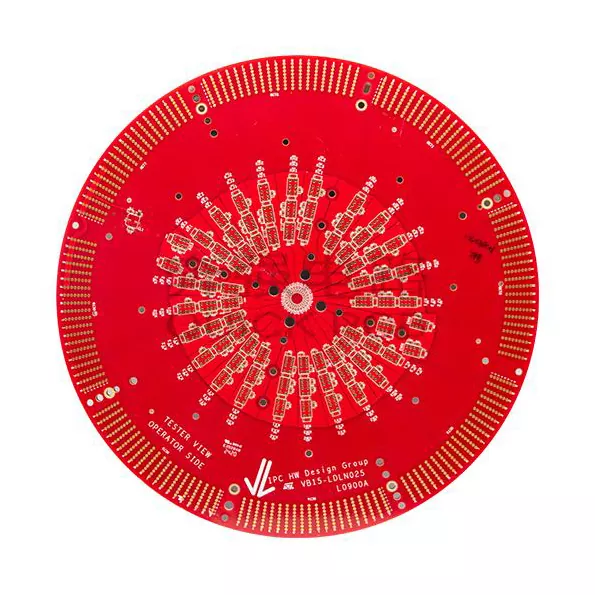
Semiconductor Testing PCB
Are you looking for reliable Semiconductor Testing PCBs arrangements that convey remarkable execution? At Aisen Electronics Co., Ltd., we get it the basic significance of exactness testing in semiconductor fabricating. Our progressed plans guarantee your electronic components meet the most noteworthy industry benchmarks whereas keeping up ideal usefulness all through their lifecycle.
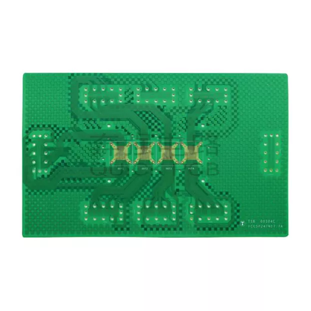
Semiconductor Packaging PCB
Shenzhen Aisen Electronics Co., Ltd. manufactures Semiconductor Packaging PCB designed for high-density semiconductor applications, supporting BGA, QFN, and flip-chip packaging requirements. With up to 32-layer capability, HDI technology, fine line routing, micro vias, and controlled impedance, our PCBs provide stable signal transmission and reliable connections for automotive electronics, industrial control, power systems, and advanced consumer devices.
As a reliable Semiconductor PCB and PCBA manufacturer and supplier in China, we have our own factory. We provide high-quality PCB manufacturing services with customized solutions for global electronic industries.