
Is a Semiconductor Testing PCB the Weak Link in Your Test Setup
Abstract: This guide from Aisen explains what makes a Semiconductor Testing PCB different from standard circuit boards, covering impedance control, contactor integration, material choice, DUT interface design, and the verification steps that prevent false test results.
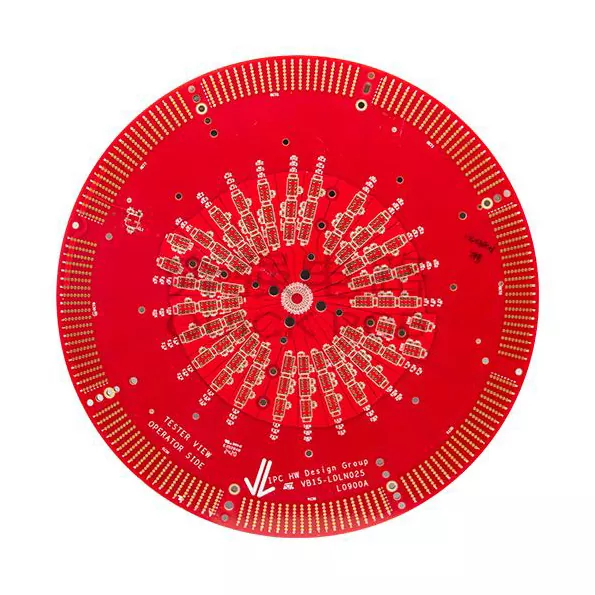
Table of Contents
- 1. Why Test Boards Are Not Standard PCBs
- 2. Impedance Control and Signal Integrity Requirements
- 3. Material Selection for High-Speed Test Boards
- 4. DUT Interface, Contactors, and Probe Design
- 5. Comparison Table: Test PCB vs. Standard PCB
- 6. Verification and Acceptance Testing
- 7. Frequently Asked Questions (FAQ)
- 8. Discuss Your Test Board Project With Aisen
1. Why Test Boards Are Not Standard PCBs
In semiconductor test, the PCB is not just a carrier—it is part of the measurement system. Aisen builds Semiconductor Testing PCB assemblies for device validation, burn-in, final test, and characterization, where small electrical variations translate directly into yield and reliability data. A board that works fine in a product prototype can produce noisy, drifting, or unrepeatable results in a test socket.
Three characteristics separate test boards from product boards: tight impedance and loss control across many parallel channels, mechanical precision at the device-under-test (DUT) interface, and dimensional stability under repeated thermal cycling. When any of these is compromised, engineers end up chasing measurement errors instead of device defects.
2. Impedance Control and Signal Integrity Requirements
Modern semiconductor test involves high-speed digital, RF, and mixed-signal channels that must be routed with predictable electrical behavior. Test board design therefore demands tighter tolerances than most commercial products.
Critical signal integrity factors:
- Controlled impedance: Single-ended and differential traces specified to tight tolerances, verified by test coupon measurement.
- Channel-to-channel skew: Equal electrical length across parallel test channels prevents timing errors in multi-site testing.
- Insertion loss and crosstalk: Low-loss dielectrics and adequate spacing between high-speed lines reduce attenuation and interference.
- Grounding strategy: Continuous reference planes, stitching vias, and low-inductance return paths are essential.
- Power delivery: Low-impedance power distribution with sufficient decoupling prevents supply droop during high-current test states.
- Via design: Back-drilled or micro-via structures reduce stub effects at high frequencies.
These parameters should be defined in the fabrication drawing and confirmed with time-domain reflectometry (TDR) or vector network analyzer measurements on representative coupons.
3. Material Selection for High-Speed Test Boards
Material choice influences electrical performance, thermal behavior, and mechanical durability. Test boards often endure thousands of insertions and repeated temperature cycles, so the substrate must hold up.
- FR-4 high-Tg: Cost-effective for lower-speed digital and burn-in boards; adequate when thermal and loss requirements are moderate.
- Modified FR-4 / mid-loss laminates: A practical middle ground when insertion loss matters but budget is constrained.
- Low-loss laminates (PTFE, hydrocarbon, or similar): Required for high-frequency and RF test where loss and phase stability are critical.
- Ceramic-filled materials: Chosen where thermal expansion must closely match the device or package.
- Copper finish: ENIG, immersion silver, or hard gold depending on contact wear, wire bonding needs, and solderability.
- Surface finish and plating thickness: Hard gold at contact pads is common where repeated insertion wear is expected.
Material selection should follow the frequency range and insertion count, not a general "premium" preference—over-specifying raises cost without improving results.
4. DUT Interface, Contactors, and Probe Design
The DUT interface is where test boards most often fail in practice. Even a well-routed board will misbehave if the socket or probe contact is misaligned or worn.
Design considerations at the interface:
- Pad geometry and position tolerance: DUT pads must align precisely with socket or probe contact positions.
- Contact wear resistance: Hard gold plating and appropriate pad thickness extend interface life.
- Planarity: Coplanarity between the board and socket affects contact resistance consistency.
- Thermal expansion matching: Mismatch between board and socket materials causes contact drift during temperature cycling.
- Mechanical fixturing: Stiffeners or metal cores reduce flexing under insertion force.
- Serviceability: Design so worn sockets or contact pins can be replaced without scrapping the whole board.
Where multi-site testing is used, channel symmetry becomes even more important—if one site has a different trace length or pad condition, its results diverge from the rest.
5. Comparison Table: Test PCB vs. Standard PCB
The table below highlights how semiconductor testing boards differ from conventional product PCBs.
| Attribute | Semiconductor Testing PCB | Standard Product PCB |
|---|---|---|
| Impedance tolerance | Tight, often ±5% or better, verified by coupon | Generally looser, ±10% common |
| Channel-to-channel matching | Equal electrical length required | Rarely specified |
| Material selection | Driven by loss, phase stability, and thermal match | Driven mainly by cost and general performance |
| Surface finish at contacts | Hard gold for wear resistance | ENIG or HASL |
| Mechanical reinforcement | Stiffeners, metal core, planarity control | Usually not required |
| Insertion cycles | Thousands to hundreds of thousands | Often a single assembly |
| Documentation | Test coupons, TDR/VNA reports, dimensional reports | Standard fabrication records |
| Typical volume | Low to medium with high mix | High volume, low mix |
Because test boards are often low-volume and highly customized, the supplier's engineering involvement during design review matters as much as manufacturing capability.
6. Verification and Acceptance Testing
Acceptance testing should be defined before fabrication begins, so both parties agree on what "passing" means.
- Impedance verification: TDR measurements on test coupons for single-ended and differential lines.
- Continuity and isolation: Electrical test of all nets, with reported open and short results.
- Dimensional inspection: Pad positions, board thickness, and planarity checked against drawings.
- Surface finish verification: Plating thickness measured at contact areas.
- Thermal cycling evaluation: Where specified, sample boards subjected to cycling before full production.
- Traceability: Material lots, process parameters, and test records retained for later reference.
Keeping baseline measurement data helps when a test cell later produces questionable results—comparing current readings to the board's original data quickly separates board drift from device failure.
7. Frequently Asked Questions (FAQ)
Q1: What is a semiconductor testing PCB used for?
A: It provides the electrical and mechanical interface between test equipment and a semiconductor device during wafer sort, final test, burn-in, characterization, or reliability testing.
Q2: Why is impedance control so important on test boards?
A: Because measurement accuracy depends on it. Uncontrolled impedance and skew introduce signal distortion that can be mistaken for device defects, producing false failures and unreliable data.
Q3: Which materials are used for high-speed test boards?
A: High-Tg FR-4 for moderate speeds, mid-loss laminates for balanced performance, and low-loss materials such as PTFE or hydrocarbon laminates for high-frequency and RF testing.
Q4: How many insertion cycles should the board withstand?
A: It depends on the test program. Burn-in and repeated final test can involve thousands of insertions, which is why hard gold contact plating and replaceable socket designs are commonly specified.
Q5: Can test boards be delivered with test reports?
A: Yes. Specify requirements for TDR or VNA coupon data, continuity and isolation results, plating thickness measurements, and dimensional inspection reports at the quotation stage.
Q6: What information is needed for a quotation?
A: Gerber files, stack-up and impedance requirements, material preference, surface finish, contact area specifications, DUT and socket details, quantity, and any acceptance criteria.
Q7: How does multi-site testing affect board design?
A: Each site must have matched electrical length, symmetrical layout, and consistent pad quality so results from all sites are comparable and can be correlated.
8. Discuss Your Test Board Project With Aisen
A semiconductor testing PCB is a precision instrument disguised as a circuit board—its value shows up in repeatable data, not in a spec sheet alone. Aisen Electronics supports PCB and PCBA projects with an engineering team that reviews stack-up, impedance targets, contactor integration, and acceptance criteria before production begins. Whether you need a single high-speed characterization board, a multi-site final test load board, or a burn-in fixture with replaceable sockets, we provide customized solutions, fast response, and reliable manufacturing support. Share your Gerber files, impedance requirements, DUT interface details, and quantity, and we will return a technical review and quotation. contact us today to discuss your test board requirements, and let our engineers help you avoid the hidden weak links—contact us now to get your project moving.
Related News
- How Can a Flow Rate And Dispensing Systems PCB Improve Fluid Measurement Accuracy and Equipment Reliability
- How Can an Electrical Muscle Stimulation Equipment PCB Improve Device Precision, Safety, and Reliability
- How Can a Converter and Selector PCB Improve Electronic Control, Reliability, and Design Flexibility
- How Can Industrial Control Instruments PCB Improve Reliability, Signal Accuracy, and Long-Term Automation Performance
- Why Is an Electrical Measuring Instruments PCB Critical for Accurate and Reliable Measurement
- How Can a Communication Routers PCB Board Improve High-Speed Network Performance and Reliability
Leave me a message