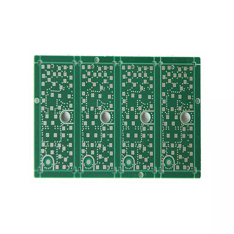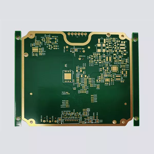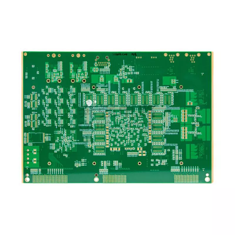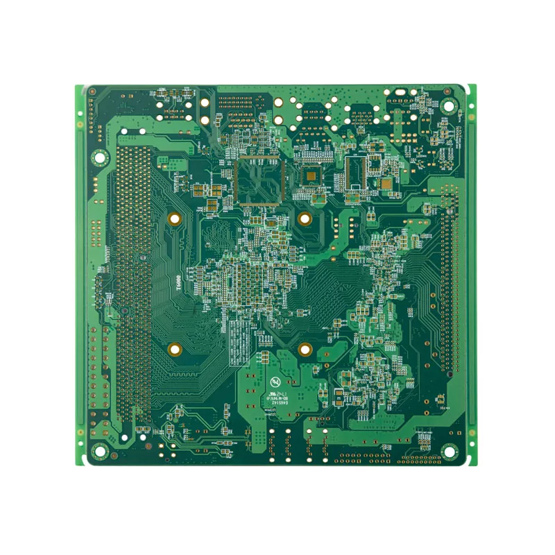

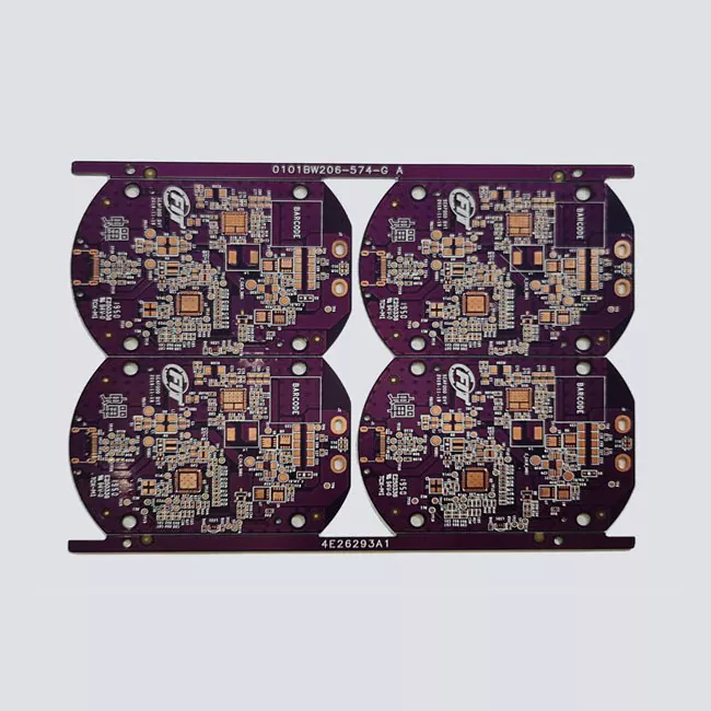
Satellite Navigation GPS PCB
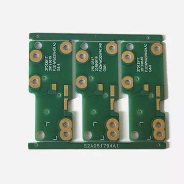
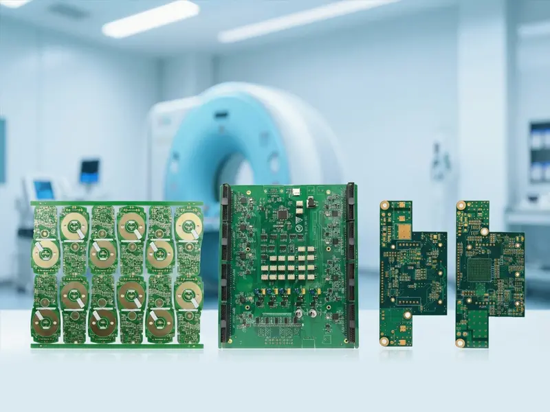
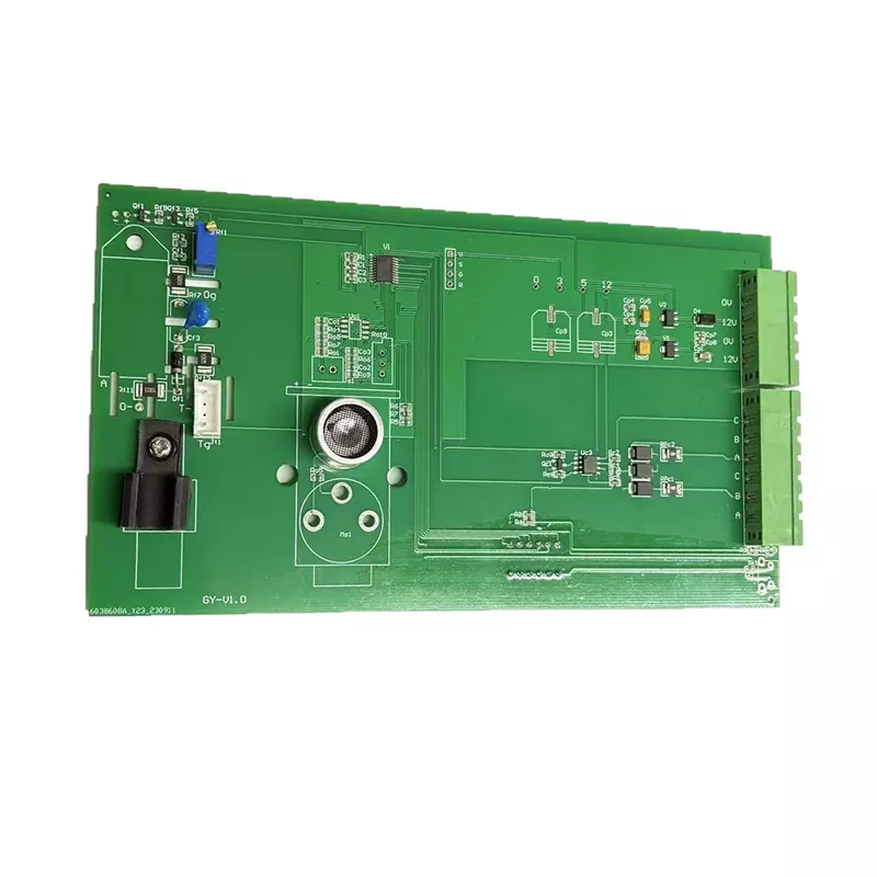
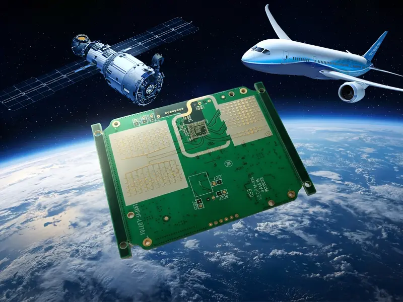
When your GPS navigation project demands precision and reliability, choosing the right Satellite Navigation GPS pcb gets to be pivotal for your victory. At Shenzhen Aisen Electronics Co., Ltd., we specialize in fabricating premium-quality route PCBs that control everything from car GPS frameworks to aviation applications. Our progressed fabricating forms guarantee your item conveys extraordinary flag judgment and long-term toughness for mission-critical route applications.
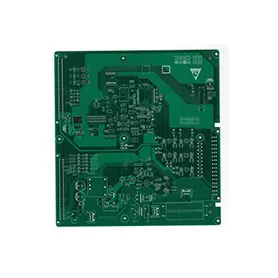
Satellite navigation systems depend on stable signal reception and accurate data processing. A GPS PCB is not only a connection platform for electronic components but also a critical part that affects antenna performance, RF transmission quality, and positioning accuracy. At Aisen Electronics Co., Ltd., we manufacture Satellite Navigation GPS PCB where signal stability, compact design, and long-term reliability are essential. Our manufacturing approach focuses on controlling electrical performance from PCB stack-up design to final inspection.
Key PCB Technologies for Satellite Navigation Applications
RF Signal Integrity and Impedance Control
GPS and GNSS systems receive extremely weak satellite signals, which means even small transmission losses can affect positioning performance.
Our GPS PCB manufacturing supports controlled impedance designs, including 50Ω RF transmission requirements commonly used in antenna and receiver circuits. Proper stack-up planning, dielectric material selection, and copper thickness control help reduce signal reflection and maintain consistent RF performance.
For high-frequency GPS applications, we work with customers to optimize:
- RF trace routing
- Ground plane design
- Return current paths
- Antenna matching areas
These factors are especially important for compact navigation devices where PCB space is limited.
HDI and Miniaturized GPS Circuit Design
Modern GPS modules are becoming smaller while integrating more functions, including multi-band positioning, wireless communication, and sensor interfaces.
Our HDI PCB capabilities allow designers to achieve higher component density through microvia technology and optimized layer structures. This helps support compact GNSS devices without sacrificing electrical performance.
Typical capabilities include:
- 1+N+1 and 2+N+2 HDI structures
- Micro vias down to 0.1mm
- Fine line and space manufacturing
- Multi-layer routing optimization
These technologies are suitable for portable navigation equipment, tracking terminals, and embedded positioning modules.
GPS PCB Manufacturing Specifications
Aisen Electronics provides flexible manufacturing options according to different navigation system requirements.
| Item | Capability |
|---|---|
| Layer Count | 1-32 layers |
| Minimum Line Width | 3mil |
| Impedance Control | ±8% tolerance |
| HDI Structure | 1+N+1 / 2+N+2 |
| Surface Finish | ENIG, OSP, Immersion Silver |
| Material Options | Standard FR4, High-frequency laminates |
| Prototype and Volume Production | Supported |
Application-Specific GPS PCB Design Considerations
Automotive Navigation PCB
Automotive GPS systems operate in environments affected by vibration, temperature changes, and electromagnetic interference.
For vehicle navigation applications, our PCB designs focus on:
- Stable signal transmission during vehicle movement
- Thermal reliability for continuous operation
- Protection against environmental moisture
- Compatibility with automotive electronic systems
These considerations help GPS modules maintain consistent positioning performance during long-term vehicle operation.
Marine and Outdoor Positioning Equipment
Marine GPS devices require stronger environmental resistance due to humidity, temperature variation, and continuous exposure to outdoor conditions.
PCB designs for these applications typically require:
- Enhanced moisture protection
- Reliable surface finishes
- Strong solder joint performance
- Stable electrical characteristics
Industrial Tracking and IoT Positioning Devices
Industrial tracking equipment often requires compact PCB designs with long operating cycles.
Our GPS PCB solutions support applications such as:
- Fleet tracking terminals
- Asset monitoring systems
- Remote positioning devices
- Smart logistics equipment
Manufacturing Process Focused on Electrical Reliability
PCB Quality Control from Material Selection to Final Testing
GPS PCB performance depends heavily on manufacturing consistency. A small variation in dielectric thickness, copper distribution, or drilling accuracy can influence RF characteristics.
Our production process includes:
Incoming Material Inspection
Raw materials are checked before production to verify specifications including laminate quality, copper thickness, and supplier compliance.
Production Process Control
During PCB fabrication, critical parameters such as drilling accuracy, layer alignment, copper thickness, and impedance requirements are monitored.
Electrical and Functional Testing
Finished boards undergo inspection procedures including AOI inspection, electrical testing, and appearance verification before shipment.
This process helps ensure each GPS PCB meets the customer's design requirements before entering final assembly.
Prototype to Mass Production Support
Different GPS projects require different manufacturing approaches. Engineering teams often need quick prototype validation before moving into large-scale production.
Aisen Electronics supports:
Prototype PCB production for early design verification
Small-batch manufacturing for market testing
Volume production for commercial navigation equipment
Our engineering team can assist with PCB manufacturability review, stack-up recommendations, and design optimization before production begins.
Engineering Support for GPS PCB Development
Successful GPS PCB projects require more than manufacturing capability. During development, our engineers support customers with:
- PCB layout review
- Stack-up recommendations
- RF design considerations
- Manufacturing feasibility analysis
- Production optimization suggestions
This helps reduce redesign risks and improves the transition from prototype to production.
Why Choose Aisen Electronics for GPS PCB Manufacturing?
Choosing a GPS PCB supplier requires evaluating not only manufacturing capacity but also technical understanding of satellite communication requirements.
Aisen Electronics Co., Ltd. combines PCB fabrication experience with engineering support to help customers develop reliable navigation products.
Our advantages include:
- Experience in multi-layer and HDI PCB manufacturing
- Capability for RF-oriented PCB designs
- Flexible support from prototypes to volume production
- Focus on signal integrity and manufacturing consistency
We work with customers to build GPS circuit boards that meet practical application requirements in automotive, marine, industrial, and consumer navigation systems.
FAQ
What type of PCB is commonly used for GPS modules?
GPS modules usually require multi-layer PCBs with controlled impedance and optimized RF routing. The PCB structure depends on antenna design, frequency requirements, and device size.
Why does GPS PCB require impedance control?
GPS signals operate at high frequencies and are sensitive to signal loss. Controlled impedance helps maintain stable RF transmission between antenna and receiver circuits.
Can GPS PCB support multi-band GNSS systems?
Yes. Satellite Navigation GPS PCB can be designed for multi-band GNSS applications, including systems using GPS, Galileo, GLONASS, and BeiDou signals.
What materials are suitable for GPS circuit boards?
Material selection depends on frequency requirements. Standard FR4 can support many applications, while high-frequency laminates are preferred for advanced RF performance.
Do you provide GPS PCB prototype manufacturing?
Yes. Aisen Electronics supports prototype development, small batch production, and volume manufacturing.
How do you test GPS PCB quality?
Testing may include AOI inspection, electrical testing, impedance verification, and manufacturing quality inspection according to project requirements.
Start Your GPS PCB Project with Aisen Electronics
If you are developing navigation equipment, GNSS modules, or positioning systems, Aisen Electronics Co., Ltd. can provide PCB manufacturing support from prototype validation to mass production.
Contact our engineering team to discuss your GPS PCB requirements, including layer structure, RF performance, material selection, and production planning.
Email: violet@akesonpcb.com
Hot Tags: Satellite Navigation GPS PCB Manufacturer, GPS PCB Supplier, Custom GPS Circuit Board
Send Inquiry
Contact Info
-
Address
3D4B QiLinXinCun.QiLinYajiu songguang Bao’an Dist, Shenzhen Guangdong Province, China
-
Tel
-
E-mail
Contact Aisen Electronics for PCB and PCBA projects. Our engineering team provides customized solutions, fast response, and reliable manufacturing support.