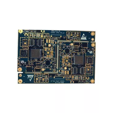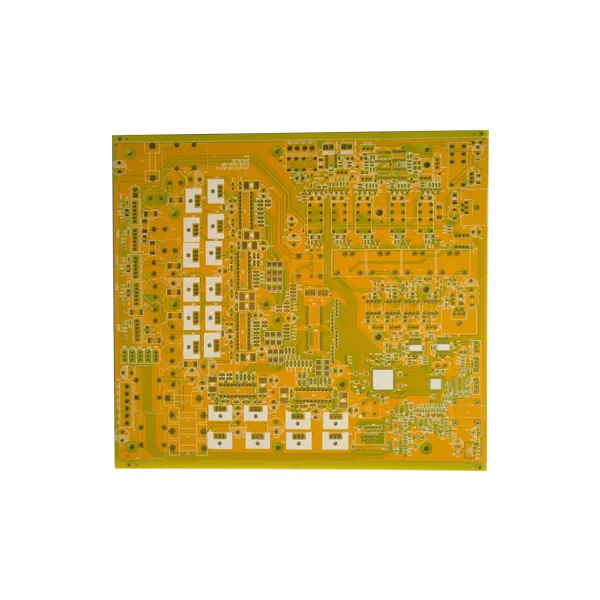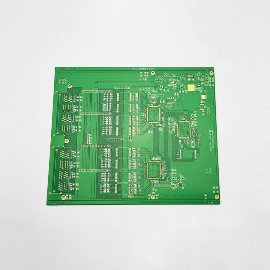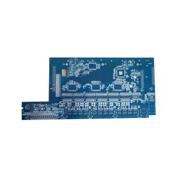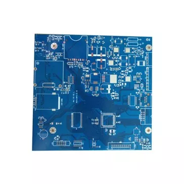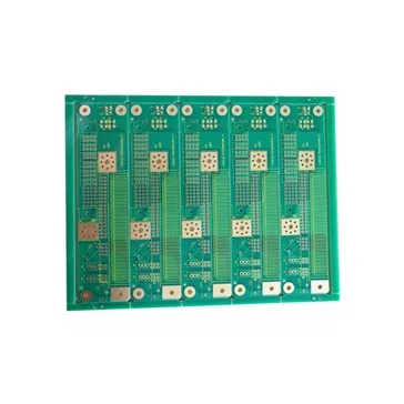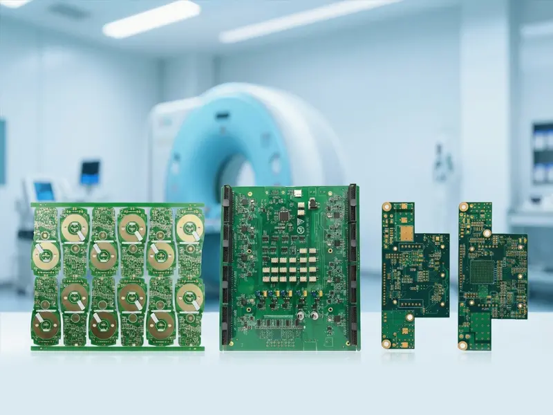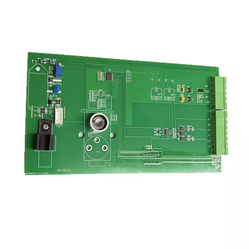

X-Ray Computed Tomography PCB
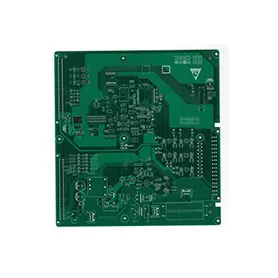
Aisen Electronics Co., Ltd. provides X-Ray Computed Tomography PCB solutions designed for medical imaging systems requiring stable signal transmission and high-density circuit integration. Our PCBs support CT sensor control, image data processing, and power management with multilayer fabrication, impedance control, HDI technology, and strict quality inspection to help medical equipment manufacturers achieve accurate and reliable imaging performance.
X-ray computed tomography systems rely on precise electronic control and stable signal processing to generate accurate diagnostic images. The PCB inside a CT scanner is not only a carrier for electronic components but also a critical platform that connects detector modules, data acquisition circuits, power management units, and control systems.
Aisen Electronics Co., Ltd. manufactures X-ray computed tomography PCB solutions designed for medical imaging equipment manufacturers requiring high-density layouts, controlled impedance, low signal interference, and consistent production quality.
Our PCB manufacturing capabilities support complex medical imaging applications, including CT detector boards, image processing control boards, power distribution boards, and embedded control modules.
PCB Design Requirements for X-Ray CT Equipment
CT imaging systems process a large amount of digital information from multiple detector channels. Any instability caused by signal loss, impedance variation, thermal stress, or electrical noise may affect image reconstruction accuracy.
Unlike standard industrial circuit boards, CT PCBs require careful control of:
- High-speed signal transmission between detector and processing units
- Low-noise circuits for sensitive analog signals
- Stable power delivery for imaging modules
- Long-term operation under continuous working conditions
- High-density component integration within limited space
Aisen Electronics works with engineers to optimize PCB structures according to application requirements, ensuring the circuit design matches the performance demands of medical imaging equipment.
High-Speed Signal Integrity for CT Detector Applications
The detector system is one of the most sensitive parts of a CT scanner. The PCB must maintain consistent electrical performance while transferring signals from multiple sensor channels.
Our manufacturing process supports:
- Controlled impedance design with ±8% tolerance
- Fine-line routing for high-density signal paths
- Low-loss material selection for high-frequency applications
- Optimized stack-up design for signal isolation
For CT systems requiring stable image data transmission, proper PCB layer configuration and impedance control help reduce signal distortion during operation.
Multi-Layer PCB Manufacturing for Complex Medical Imaging Systems
Modern CT equipment integrates thousands of electronic connections into compact assemblies. Multi-layer PCB structures provide the routing space required for complex signal, power, and grounding networks.
Aisen Electronics manufactures:
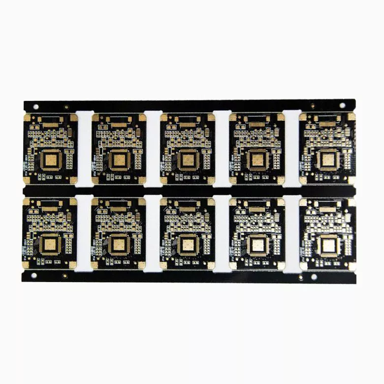
- 4-layer to 32-layer rigid PCBs
- HDI PCB structures
- Micro-via and blind via designs
- High-density BGA component layouts
Technical capabilities include:
| Parameter | Capability |
|---|---|
| Minimum line width/spacing | 0.076mm / 3mil |
| Minimum micro via size | 0.1mm |
| BGA package support | Down to 0.22mm pad diameter |
| Maximum copper thickness | Up to 6oz |
| Board thickness | 0.3mm - 5.0mm |
| Maximum board size | 810mm × 490mm |
These capabilities allow CT manufacturers to integrate compact control circuits while maintaining electrical performance.
Materials Selection for Medical Imaging PCB Applications
The material selection directly affects signal stability, thermal performance, and service life.
Depending on CT system requirements, Aisen Electronics provides:
High Tg Materials
Suitable for equipment operating under continuous load conditions. Higher glass transition temperatures improve dimensional stability during manufacturing and operation.
Low-Loss PCB Materials
Used for high-speed signal transmission where dielectric characteristics influence signal accuracy.
Heavy Copper PCB Structures
Copper thickness up to 6oz supports applications requiring higher current capacity and improved thermal dissipation.
Material selection is evaluated based on operating frequency, power requirements, board structure, and environmental conditions.
Manufacturing Process Control for Medical PCB Production
Medical imaging equipment requires consistent production quality because PCB failure can affect the entire diagnostic system.
Aisen Electronics applies quality checkpoints throughout manufacturing:
Incoming Material Inspection
All incoming laminates, copper materials, and components are checked according to production requirements before entering manufacturing.
Manufacturing Process Monitoring
Critical processes including drilling, lamination, copper plating, imaging, and surface finishing are monitored through in-process inspections.
Electrical Performance Testing
Finished boards undergo electrical testing to verify:
- Open and short circuit performance
- Signal connection reliability
- Layer-to-layer conductivity
Final Quality Inspection
Before shipment, each batch is inspected according to customer specifications, including appearance inspection, dimensional verification, and packaging confirmation.
Surface Finishing Options for CT PCB Assembly
Medical imaging equipment requires stable solder connections and long-term component reliability.
Aisen Electronics provides several surface treatment options:
ENIG (Electroless Nickel Immersion Gold)
Provides excellent solderability and corrosion resistance, commonly used for high-density component assembly.
OSP Surface Treatment
Suitable for applications requiring flat copper surfaces and lead-free assembly compatibility.
Immersion Silver
Used for applications requiring good electrical performance and soldering reliability.
Surface treatment selection depends on assembly process, storage requirements, and component type.
PCBA Assembly Capability for Medical Imaging Electronics
Besides PCB fabrication, Aisen Electronics provides PCB assembly services for medical imaging manufacturers.
Our assembly capability includes:
- 01005 miniature components
- Fine-pitch BGA packages
- Mixed SMT and through-hole assembly
- Automated optical inspection (AOI)
- X-ray inspection for hidden solder joints
Assembly parameters:
| Item | Capability |
|---|---|
| Minimum component pitch | 0.38mm |
| Placement accuracy | ±0.025mm |
| Solder paste thickness control | ±0.03mm |
| Maximum component height | 13mm |
This integrated manufacturing approach helps reduce communication costs between PCB fabrication and assembly stages.
Production Lead Time for CT PCB Projects
Medical equipment manufacturers often require predictable production schedules for prototype validation and mass production.
Typical lead times:
| PCB Type | Prototype | Mass Production |
|---|---|---|
| 4-layer PCB | 3-4 working days | 10-12 working days |
| 6-layer PCB | 5-6 working days | 12-14 working days |
| 8+ layer PCB | According to structure complexity | Customized schedule |
Actual delivery time depends on material availability, PCB structure, quantity, and testing requirements.
Why Medical Imaging Companies Choose Aisen Electronics
Selecting a PCB supplier for CT equipment requires more than manufacturing capacity. Engineering support, process control, and production consistency directly influence the reliability of the final medical device.
Aisen Electronics Co., Ltd. supports medical imaging manufacturers with:
- Experience in complex multi-layer PCB production
- HDI and high-density interconnection capability
- Controlled impedance manufacturing processes
- Complete PCB and PCBA services
- Flexible support from prototype development to volume production
We work with equipment manufacturers to develop PCB solutions that meet the electrical and mechanical requirements of modern CT imaging systems.
Frequently Asked Questions About X-Ray Computed Tomography PCB
What type of PCB is used in X-ray CT scanners?
CT scanners typically use multi-layer rigid PCBs, HDI PCBs, and specialized control boards for detector modules, image processing units, and power management systems.
Why does CT equipment require high-density PCB designs?
CT systems contain multiple electronic modules in limited installation space. High-density PCB technology allows more signal channels and components to be integrated while maintaining routing performance.
How does PCB quality affect CT image performance?
PCB design influences signal transmission stability, electrical noise control, and data processing accuracy. Poor PCB performance may affect system reliability and imaging consistency.
Can Aisen Electronics manufacture prototype CT PCBs?
Yes. Aisen Electronics supports prototype production and volume manufacturing with different layer counts, materials, and surface finishes.
What PCB testing methods are available?
Testing includes electrical testing, AOI inspection, dimensional inspection, and manufacturing process verification based on customer requirements.
Does Aisen Electronics provide PCB assembly services?
Yes. We provide PCBA assembly including SMT placement, inspection, and finished board delivery.
Contact Aisen Electronics for X-Ray CT PCB Manufacturing
If you are developing medical imaging equipment and need PCB solutions for CT systems, Aisen Electronics Co., Ltd. can provide manufacturing support based on your electrical, mechanical, and production requirements.
Contact our engineering team to discuss PCB specifications, prototype requirements, and production plans.
Hot Tags: X-Ray CT PCB Manufacturer, X-Ray Computed Tomography PCB Supplier, Customized CT PCB
Send Inquiry
Contact Info
-
Address
3D4B QiLinXinCun.QiLinYajiu songguang Bao’an Dist, Shenzhen Guangdong Province, China
-
Tel
-
E-mail
Contact Aisen Electronics for PCB and PCBA projects. Our engineering team provides customized solutions, fast response, and reliable manufacturing support.