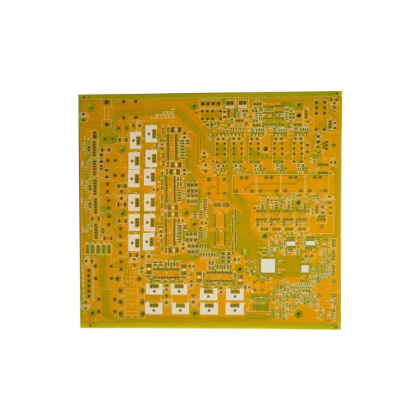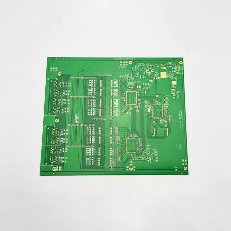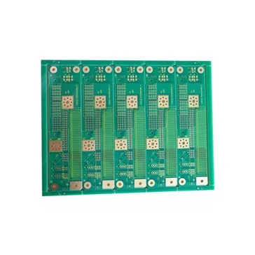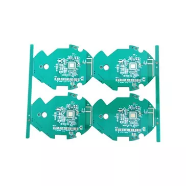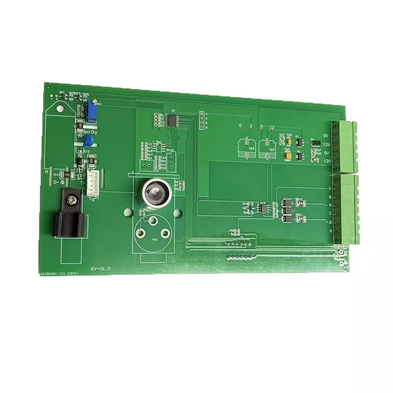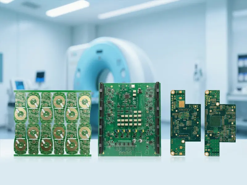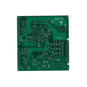

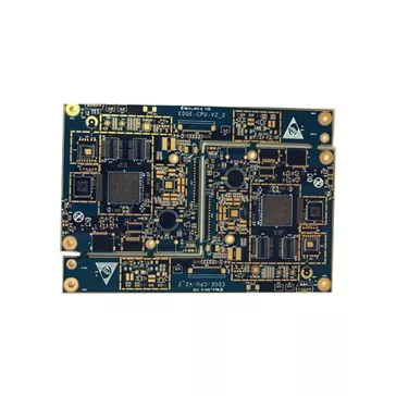
Implantable Medical Devices PCB
When your medical device needs to function flawlessly inside the human body, you need Implantable Medical Devices pcb that meet the most noteworthy measures of quality and unwavering quality. At Shenzhen Aisen Electronics Co., Ltd.., we get it that these specialized circuit sheets are actually things of life and passing. Each follow, each through, and each component situation must be culminate. Your patients depend on it, and we provide the exactness you require for basic therapeutic applications.
Implantable medical devices require circuit boards that can maintain stable electrical performance while operating inside the human body for extended periods. Unlike standard electronic products, implantable devices must withstand strict environmental conditions, limited installation space, and continuous operation requirements.
The PCB inside an implantable medical device supports critical functions such as signal processing, power management, communication, and system control. Aisen Electronics Co., Ltd. manufactures Implantable Medical Devices PCB with a focus on miniaturized design, material reliability, precise manufacturing control, and consistent electrical performance for advanced healthcare applications.
What Makes Implantable Medical Device PCBs Different?
Designed for Long-Term Operation Inside the Human Body
Implantable electronics may operate for years without direct maintenance, making PCB reliability a key factor in overall device performance.
The circuit board must maintain stable connections while facing challenges such as moisture exposure, temperature variation, limited airflow, and continuous electrical stress. PCB materials, surface finishes, and manufacturing processes all influence the service life of the final medical device.
Aisen Electronics evaluates PCB structures according to application requirements, helping customers select suitable materials, layer configurations, and manufacturing processes for different implantable systems.
Miniaturization Without Compromising Electrical Performance
Many implantable devices require compact dimensions while integrating more electronic functions. Pacemakers, drug delivery systems, neural implants, and monitoring devices all require high circuit density within very limited spaces.
Through HDI technology and advanced multilayer manufacturing, Aisen Electronics supports smaller PCB designs with complex routing requirements. Fine-line fabrication, microvia structures, and high-density component integration help engineers achieve compact device layouts while maintaining electrical stability.
PCB Technology for Implantable Medical Applications
High-Density Interconnect for Compact Medical Electronics
Modern implantable devices continue to become smaller while requiring more processing capability. Traditional PCB structures may not provide enough routing space for these designs.
Aisen Electronics supports Implantable Medical Devices PCB manufacturing with microvia technology, fine-line circuits, and multilayer structures up to 32 layers. These capabilities allow designers to integrate control circuits, communication modules, and power management systems into smaller medical devices.
Material Selection for Medical Device Reliability
Material selection plays an important role in implantable PCB performance. The board structure must maintain stable electrical properties throughout the expected operating lifetime of the device.
Depending on application requirements, Aisen Electronics works with customers to evaluate factors such as signal frequency, thermal conditions, mechanical requirements, and long-term reliability. Surface finishes including ENIG can be selected to improve solder performance and corrosion resistance.
Manufacturing Capabilities for Implantable Medical Device PCBs
Precision Fabrication for Complex Medical Circuits
Implantable medical electronics require tighter manufacturing control compared with many commercial electronic products.
Aisen Electronics provides multilayer PCB manufacturing with capabilities including fine-line processing, precision drilling, controlled impedance fabrication, and high-density interconnection technology.
Key manufacturing capabilities include:
| Parameter | Capability |
|---|---|
| Layer Count | 1-32 Layers |
| Minimum Line Width/Spacing | 3mil/3mil |
| Minimum Via Size | 0.1mm |
| Board Thickness | 0.3-5.0mm |
| Copper Thickness | Up to 6oz |
| Hole Copper Thickness | ≥25μm |
| Impedance Control | ±8% |
PCB Manufacturing Process
Controlled Production from Prototype to Mass Production
Consistency is essential for medical electronics because PCB performance directly affects the reliability of the finished device.
Aisen Electronics controls the complete manufacturing process, including material inspection, inner layer production, lamination, drilling, copper plating, circuit imaging, surface treatment, electrical testing, and final inspection.
Each production stage is monitored to reduce variation and maintain stable performance between development samples and production batches.
Testing and Quality Verification
Before shipment, implantable medical device PCBs undergo inspection procedures designed to verify electrical and manufacturing performance.
Testing includes automated optical inspection, electrical testing, impedance verification, dimensional inspection, and final quality checks. These processes help identify manufacturing defects before boards are assembled into medical equipment.
PCBA Assembly Support for Implantable Medical Electronics
Precision Assembly for Compact Healthcare Devices
Implantable devices often require highly integrated PCB assemblies with miniature components and strict placement accuracy.
Aisen Electronics provides PCBA assembly services supporting fine-pitch components, miniature packages, BGA assembly, and automated inspection. Combining PCB fabrication and assembly helps medical device manufacturers simplify production management and improve manufacturing consistency.
Engineering Support for Implantable Device PCB Development
Helping Optimize Designs Before Manufacturing
The PCB development stage has a significant impact on the final device size, reliability, and production efficiency.
Aisen Electronics works with medical device engineers to review PCB layouts, stack-up structures, routing methods, component placement, and manufacturability. Early design communication helps identify potential issues before production begins.
Applications of Implantable Medical Device PCBs
Supporting Different Types of Medical Implant Electronics
Implantable PCB technology is used across various healthcare applications where long-term electronic stability is required.
Typical applications include cardiac implants, neural stimulation systems, drug delivery devices, implantable monitoring equipment, and other medical electronics requiring compact and dependable circuit solutions.
Each application has different electrical and mechanical requirements, making PCB design and manufacturing customization essential.
Why Choose Aisen Electronics Co., Ltd. for Implantable Medical Device PCB Manufacturing?
Implantable medical electronics require more than compact circuit design. They require manufacturing processes that support long-term reliability, stable electrical performance, and consistent quality throughout the product lifecycle.
Aisen Electronics Co., Ltd. combines multilayer PCB manufacturing, HDI technology, precision assembly, and quality control experience to support medical device companies developing next-generation implantable products.
From prototype development to volume production, we provide PCB solutions tailored to the technical requirements of implantable healthcare systems.
Frequently Asked Questions
What PCB technology is commonly used for implantable medical devices?
Implantable medical devices commonly use multilayer PCBs, HDI structures, and compact circuit designs to integrate multiple electronic functions within limited space.
Why are Implantable Medical Devices PCB different from standard circuit boards?
They require longer operational stability, tighter manufacturing control, smaller dimensions, and materials suitable for demanding medical environments.
Can implantable medical PCB designs be customized?
Yes. PCB layer structure, materials, routing design, and manufacturing processes can be adjusted according to different medical device requirements.
What testing is performed for implantable medical PCBs?
Testing typically includes electrical verification, optical inspection, impedance testing, dimensional checks, and manufacturing traceability review.
Discuss Your Implantable Medical PCB Project with Aisen Electronics Co., Ltd.
Developing implantable medical electronics requires close cooperation between device designers and PCB manufacturing engineers. Whether you are working on a new implantable system prototype or preparing for volume production, Aisen Electronics Co., Ltd. can support your project with PCB design evaluation, manufacturing recommendations, and production solutions.
Our engineering team can review your PCB requirements, including layer structure, material selection, signal integrity considerations, miniaturization needs, and assembly requirements, helping you develop a circuit solution suitable for long-term medical applications.
Contact Aisen Electronics Co., Ltd. to discuss your implantable medical device PCB requirements.
Email: violet@akesonpcb.com
We provide technical support from initial PCB design review through prototype development and production manufacturing, helping medical device companies build reliable electronic systems for next-generation healthcare applications.
Hot Tags: Implantable Medical Devices PCB Manufacturer, Medical Device PCB Supplier, Custom Medical PCB
Send Inquiry
Contact Info
-
Address
3D4B QiLinXinCun.QiLinYajiu songguang Bao’an Dist, Shenzhen Guangdong Province, China
-
Tel
-
E-mail
Contact Aisen Electronics for PCB and PCBA projects. Our engineering team provides customized solutions, fast response, and reliable manufacturing support.