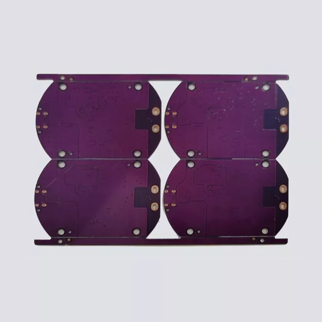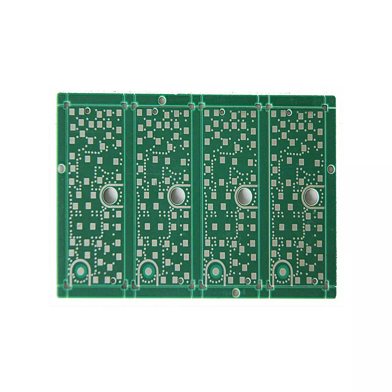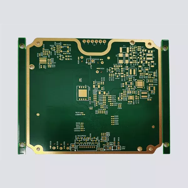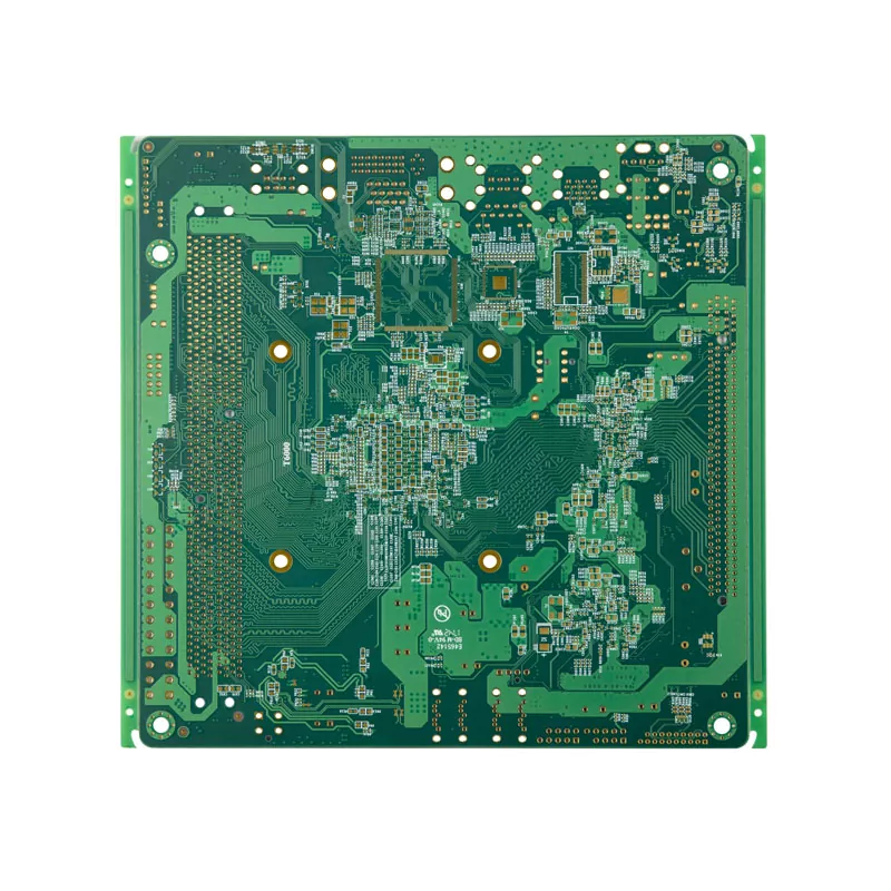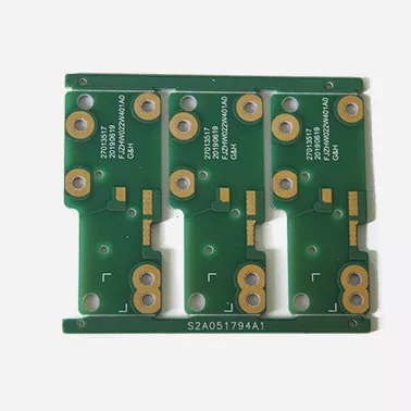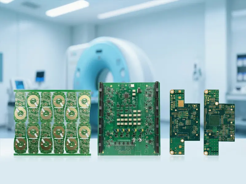

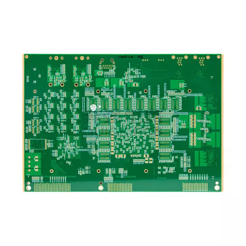
Spacecraft Communication PCB
When you're designing next-generation space missions, you need Spacecraft communication pcb arrangements that convey outright unwavering quality in the harshest situations. At Shenzhen Aisen Electronics Co., Ltd., we get it that communication frameworks are the help of any shuttle. Our progressed fabricating capabilities guarantee your item meets the thorough requests of space investigation, from introductory flag transmission to profound space communications.
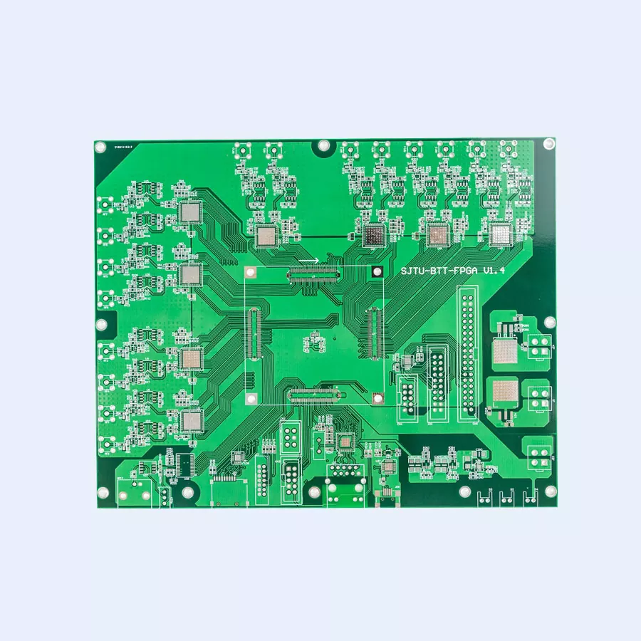
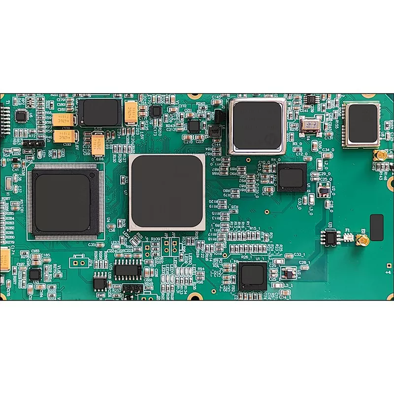
Spacecraft communication systems depend on stable electronic circuits to transmit commands, receive signals, and transfer mission data between satellites and ground stations. Inside these systems, the PCB is not only a connection platform but also a key component that determines signal quality, power distribution efficiency, and long-term operating stability.
Aisen Electronics Co., Ltd. develops spacecraft communication PCBs for satellite communication modules, RF transceivers, telemetry equipment, and onboard data processing units where electrical performance must remain consistent throughout years of operation.
Unlike conventional industrial circuit boards, spacecraft communication PCBs face unique engineering challenges. They must maintain signal integrity under vacuum conditions, tolerate temperature cycling, withstand launch vibration, and operate without physical maintenance after deployment.
The Role of PCB in Spacecraft Communication Systems
A spacecraft communication system usually contains antenna modules, RF circuits, signal processors, power management units, and data interfaces.
The communication PCB provides the electrical pathway between these components.
During operation, received radio-frequency signals are processed through communication circuits, converted into digital information, and transmitted to onboard processors or ground communication systems. Any variation in impedance, material performance, or circuit structure may affect transmission efficiency and signal accuracy.
For this reason, spacecraft communication PCB design requires careful control of:
- High-frequency signal transmission
- Electromagnetic interference
- Power distribution stability
- Thermal expansion consistency
- Long-term material reliability
High-Frequency PCB Design for Space Communication Applications
Space communication equipment often operates at high frequencies where even small signal losses can reduce communication efficiency.
Aisen Electronics Co., Ltd. supports PCB manufacturing processes designed for RF and microwave applications, including controlled impedance routing, optimized layer stack-up design, and low-loss material solutions.
Our engineering approach focuses on maintaining stable electrical characteristics through:
Precise impedance control for RF signal paths
Optimized transmission line design
Reduced signal reflection and insertion loss
Controlled dielectric performance
Stable grounding structures for EMI reduction
These technologies help communication modules maintain reliable data transmission during satellite operation.
Multilayer PCB Structures for Compact Space Electronics
Spacecraft electronic systems require high functionality within limited installation space. Multilayer PCB technology allows engineers to integrate more circuits while maintaining compact dimensions.
Aisen Electronics supports multilayer PCB manufacturing from 1 to 32 layers, including complex stack-up designs for communication modules.
Manufacturing capability includes:
- PCB layer count: 1-32 layers
- Maximum panel size: 650mm × 750mm
- Board thickness: 0.4mm-5.0mm
- Copper thickness: up to 6 OZ
- Minimum via size: 0.1mm
- Minimum line width/spacing: 3/3mil
For advanced satellite electronics requiring higher routing density, HDI structures can improve connection efficiency while reducing PCB size and weight.
HDI Technology for Lightweight Satellite Communication Modules
Weight reduction is an important consideration in spacecraft design because every additional gram increases launch cost.
HDI PCB technology allows designers to create compact communication circuits through laser microvias, fine-line routing, and optimized layer connections.
Aisen Electronics provides HDI PCB solutions supporting:
- 1+N+1 structures
- 2+N+2 structures
- Laser microvia technology
- Fine-pitch BGA component assembly
- High-density signal routing
These structures help engineers achieve smaller communication modules without sacrificing electrical performance.
Material Selection for Vacuum and Extreme Temperature Conditions
Spacecraft communication PCBs operate in environments where heat transfer and temperature control are very different from ground applications.
Without air circulation in space, PCB materials must maintain dimensional stability during repeated temperature changes.
Material selection is based on application requirements such as:
- Dielectric properties
- Thermal expansion characteristics
- Frequency performance
- Mechanical stability
Aisen Electronics supports material solutions suitable for high-frequency communication applications, helping reduce risks caused by dielectric variation and thermal expansion mismatch.
Thermal Management Design for Space Communication PCBs
Communication modules generate heat through RF components, processors, and power circuits.
Because spacecraft cannot rely on traditional cooling methods, PCB thermal design becomes important for maintaining stable operation.
Thermal management considerations include:
- Optimized copper distribution
- Thermal via structures
- Layer stack-up design
- Material compatibility evaluation
Proper thermal design helps reduce temperature-related stress during long-duration missions.
Manufacturing Process Control for Space Communication PCB Production
Aisen Electronics Co., Ltd. applies controlled manufacturing procedures to reduce variation during PCB production.
The manufacturing process includes:
Material inspection
Inner layer fabrication
Precision drilling
Copper plating
Circuit imaging
AOI inspection
Surface finishing
Electrical testing
Final inspection
For spacecraft communication applications, production traceability and process consistency are essential because electronic modules may operate for years without replacement.
Testing Requirements for Space Communication PCB Reliability
Before integration into communication equipment, PCBs require electrical and manufacturing verification.
Testing support includes:
Electrical continuity testing
Insulation resistance testing
AOI inspection
Impedance verification
Solder quality inspection
Thermal cycling evaluation according to project requirements
These inspection procedures help identify manufacturing risks before PCB assembly and system integration.
Applications
Aisen Electronics manufactures PCB solutions used in various space communication electronics, including:
Satellite communication transceivers
Telemetry and tracking systems
RF communication modules
Antenna control units
Onboard data processing equipment
Communication payload electronics
Each application requires different PCB structures depending on frequency range, power requirements, and mission objectives.
Engineering Support for Space Communication PCB Development
Space communication projects often require PCB manufacturers to participate during the design stage.
Aisen Electronics provides engineering support including:
PCB stack-up recommendations
Material selection assistance
Manufacturing feasibility review
Signal integrity considerations
DFM analysis
Early engineering communication helps customers reduce production risks and improve design manufacturability.
Why Choose Aisen Electronics Co., Ltd. for Spacecraft Communication PCB Manufacturing
Space communication PCB production requires experience in both PCB manufacturing and high-frequency electronic requirements.
Aisen Electronics Co., Ltd. combines multilayer PCB manufacturing capability, HDI technology, impedance control experience, and process management to support satellite and aerospace communication projects.
From prototype development to production manufacturing, we work with customers to develop PCB solutions that meet the electrical, mechanical, and environmental requirements of space communication systems.
FAQ
What is a spacecraft communication PCB used for?
A spacecraft communication PCB connects RF circuits, processors, power systems, and communication interfaces inside satellite communication equipment. It supports signal processing, data transmission, and system control functions.
Why do spacecraft communication PCBs require impedance control?
High-frequency communication signals are sensitive to impedance changes. Proper impedance control helps reduce signal reflection and maintain stable transmission performance.
What PCB materials are suitable for satellite communication applications?
Material selection depends on frequency requirements, thermal conditions, and reliability targets. High-frequency low-loss materials are commonly considered for RF communication circuits.
Can Aisen Electronics manufacture HDI spacecraft PCBs?
Yes. Aisen Electronics supports HDI PCB structures including laser microvias and high-density routing for compact communication modules.
Do you support prototype and small batch space PCB production?
Yes. We support prototype development, engineering verification, and production manufacturing according to project requirements.
Contact Aisen Electronics Co., Ltd.
For spacecraft communication PCB projects requiring high-frequency performance, multilayer manufacturing capability, and engineering support, contact Aisen Electronics Co., Ltd.
Email: violet@akesonpcb.com
Hot Tags: Spacecraft Communication PCB China Manufacturer, Space Communication PCB Supplier, Aerospace PCB Factory, Custom Spacecraft PCB
Send Inquiry
Contact Info
-
Address
3D4B QiLinXinCun.QiLinYajiu songguang Bao’an Dist, Shenzhen Guangdong Province, China
-
Tel
-
E-mail
Contact Aisen Electronics for PCB and PCBA projects. Our engineering team provides customized solutions, fast response, and reliable manufacturing support.