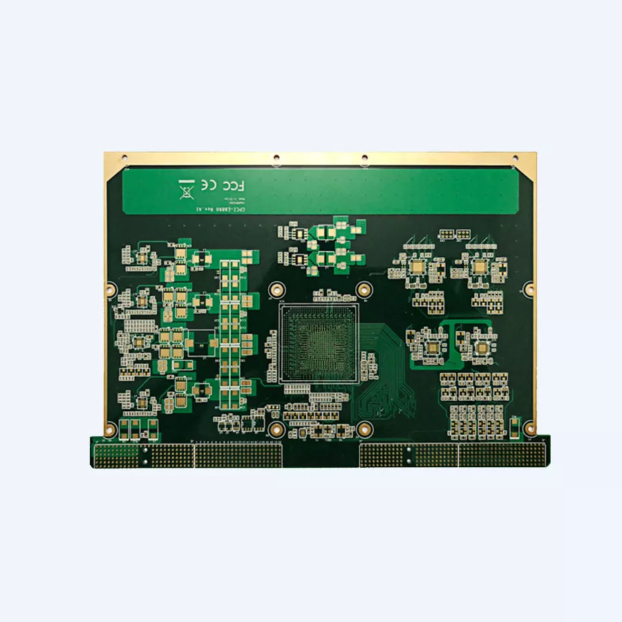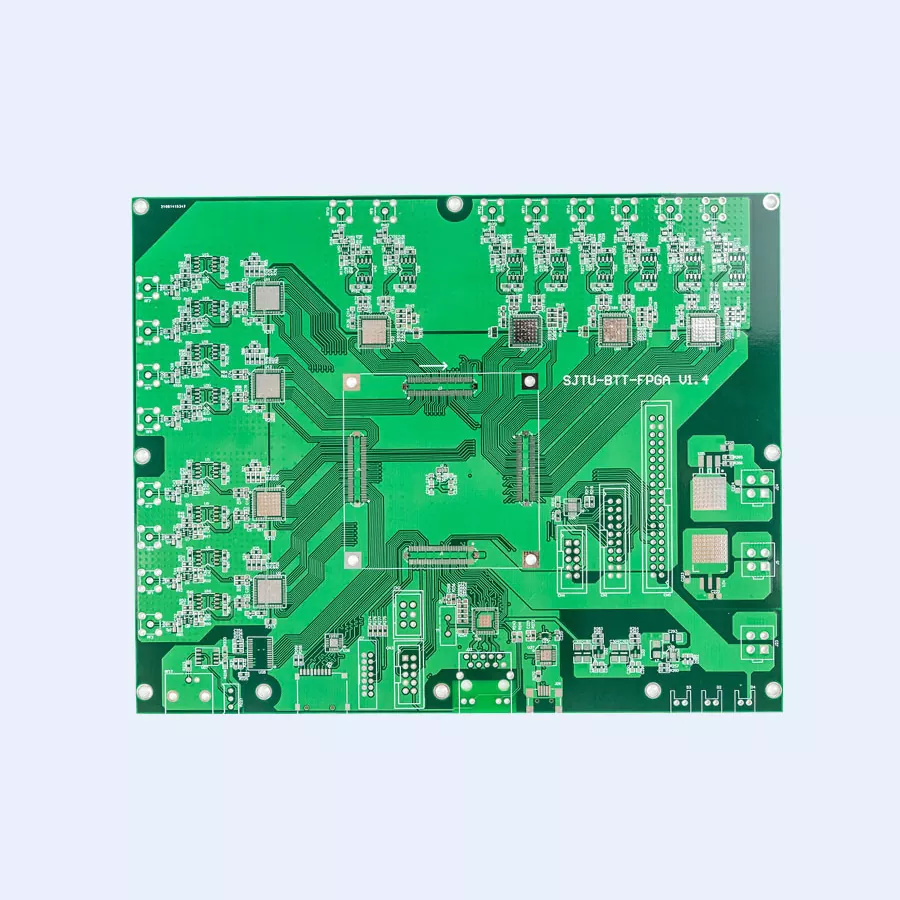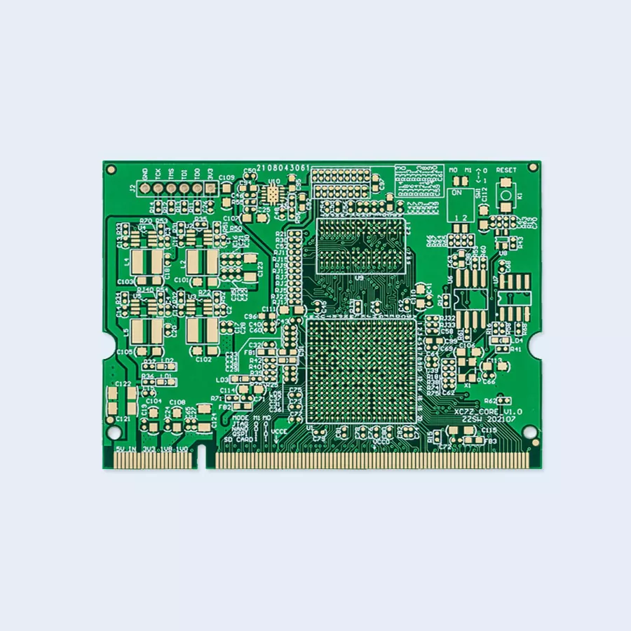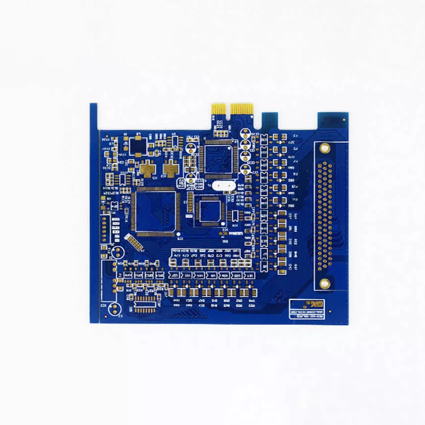
Communication Switches PCB Board
When your project demands exceptional reliability and precision, our communication switches pcb board fabricating administrations convey the quality you require. We specialize in making high-performance sheets that control today's progressed communication foundation. Whether you're creating organize gear, IoT gadgets, or complex communication frameworks, our ability guarantees your communication switches meets the most noteworthy industry standards.
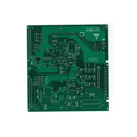
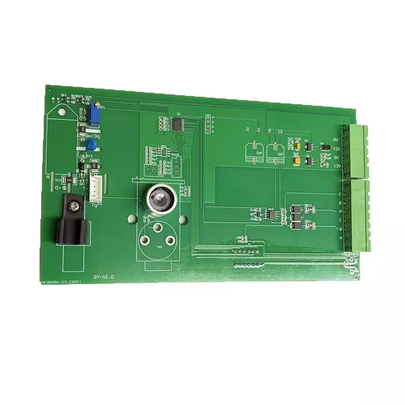
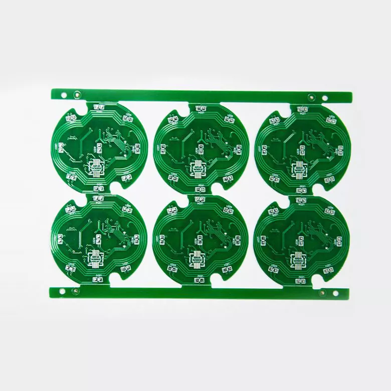
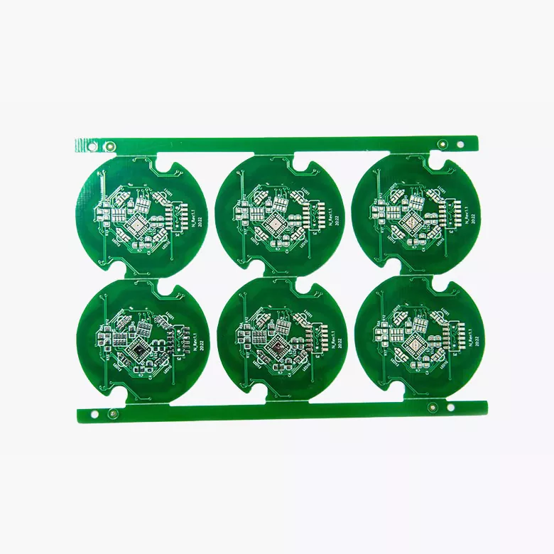
A Communication Switches PCB Board is responsible for connecting processors, switching chips, memory modules, and multiple communication interfaces inside network equipment.
Unlike ordinary electronic control boards, switch PCBs need to handle large amounts of data transmission while maintaining signal quality between multiple channels. Any signal loss, interference, or impedance variation may affect network stability.
Aisen Electronics focuses on PCB manufacturing solutions that support high-speed communication, compact layouts, and long-term operating reliability.
Key Design Requirements for Communication Switch PCB Boards
High-Speed Signal Transmission
Network switches rely on high-frequency signals to transfer data between multiple ports. The PCB structure directly influences transmission quality.
Aisen Electronics applies controlled impedance design, optimized layer stackups, and precise routing processes to reduce signal reflection and transmission loss.
These technologies are especially important for switches supporting higher Ethernet speeds and advanced communication protocols.
Multi-Port Circuit Integration
A switch PCB usually integrates multiple Ethernet ports, switching controllers, power circuits, and management modules within limited board space.
High-density PCB manufacturing allows designers to arrange complex circuits while maintaining reliable electrical connections.
Our capabilities support:
| Specification | Capability |
|---|---|
| Layer Count | 1-32 Layers |
| Minimum Line Width/Spacing | 3/3 mil |
| PCB Thickness | 0.3mm-5.0mm |
| Copper Thickness | Up to 6 OZ |
| Micro Via Capability | Down to 0.1mm |
| Impedance Control | ±8% Special Capability |
These capabilities support both compact industrial switches and high-performance network equipment.
Communication Switch PCB Compared with Other Network PCBs
Different networking products have different PCB priorities.
| PCB Type | Main Function | Main Design Focus |
|---|---|---|
| Communication Switch PCB | Data forwarding and multi-port switching | Signal integrity, port density, stable transmission |
| Router PCB | Network management and data processing | Processor integration, wireless communication |
| Gateway PCB | Protocol conversion and device connection | Interface compatibility, communication modules |
| IoT Device PCB | Small-scale data collection and transmission | Miniaturization, low power consumption |
Compared with general communication boards, switch PCBs place greater emphasis on high-speed signal routing and multi-channel communication stability.
PCB Manufacturing Process for Communication Switch Applications
Aisen Electronics controls the complete manufacturing process to maintain consistency in complex switch PCB production.
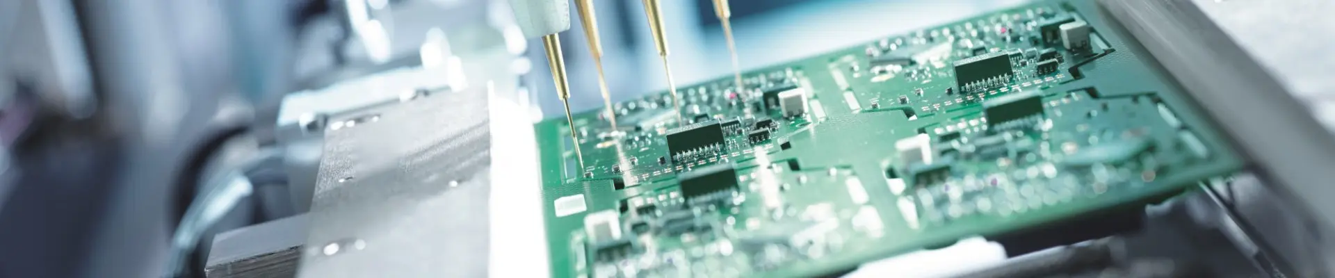
For multilayer switch boards, production includes inner layer formation, precision drilling, copper plating, circuit pattern processing, surface treatment, AOI inspection, and electrical testing.
During assembly, component placement accuracy is carefully controlled because switch boards often contain high-performance processors, memory devices, and communication chips.
The complete process helps ensure reliable connections and stable operation in network environments.
Thermal and Reliability Considerations for Network Switch PCB Boards
Communication switches often operate continuously in data centers, industrial environments, and enterprise networks.
Long operating hours create thermal challenges, especially around switching chips and power management components.
PCB design must consider:
- Copper distribution
- Heat dissipation paths
- Component placement
- Power circuit stability
Aisen Electronics works with customers to optimize PCB structures according to operating conditions and product requirements.
Surface Treatment Options for Communication Switch PCBs
Different switch designs require different surface finishes based on component type and production requirements.
ENIG is commonly selected for boards with fine-pitch components and higher reliability requirements. OSP provides a practical option for cost-sensitive designs, while HASL remains suitable for conventional electronic assemblies.
Aisen Electronics helps customers select suitable surface treatments according to assembly process and product lifetime requirements.
Communication Switch PCB Assembly Capability
Aisen Electronics provides complete PCB assembly services for communication switch manufacturers.
Our assembly capability covers fine-pitch components, complex IC packages, and high-density layouts used in modern networking products.
The service includes component sourcing, SMT assembly, inspection, and functional testing, helping customers simplify production management and improve manufacturing efficiency.
Quality Control for Communication Switch PCB Manufacturing
Network switches are often installed in critical communication environments where unexpected downtime can affect connected systems.
To maintain production consistency, Aisen Electronics applies quality control throughout the manufacturing process, including material inspection, process monitoring, AOI inspection, electrical testing, and final verification.
Each production batch is reviewed according to customer specifications before shipment.
Applications of Communication Switch PCB Boards
Aisen Electronics provides PCB solutions for various switching applications, including:
| Application | Typical Use |
|---|---|
| Ethernet Switches | Enterprise and commercial networking |
| Industrial Switches | Factory automation and industrial communication |
| PoE Switches | Network devices requiring power and data transmission |
| Data Communication Equipment | High-speed network infrastructure |
| Smart Security Systems | Video and surveillance network connections |
Engineering Support for Communication Switch PCB Development
Switch PCB development requires cooperation between electronic engineers and manufacturing specialists.
Aisen Electronics provides support during product development, including PCB design review, manufacturing feasibility analysis, stackup recommendations, and production optimization.
This helps customers reduce manufacturing risks and improve the transition from prototype to volume production.
FAQ
What is a communication switch PCB board?
A communication switch PCB board is the main circuit platform inside network switches, connecting switching chips, ports, processors, and power management systems for data transmission.
Why are switch PCBs different from normal communication PCBs?
Switch PCBs handle multiple communication channels simultaneously, requiring stronger signal integrity control, higher routing density, and stable long-term operation.
Can you manufacture multilayer switch PCB boards?
Yes. Aisen Electronics supports multilayer PCB manufacturing from simple structures to complex 32-layer designs.
Do switch PCB boards require impedance control?
Yes. Controlled impedance is important for maintaining signal quality in high-speed Ethernet and communication applications.
Can you provide PCB assembly for communication switches?
Yes. We provide complete PCBA services including component sourcing, SMT assembly, inspection, and testing.
What information is needed for a switch PCB quotation?
Customers can provide Gerber files, BOM files, PCB specifications, required quantity, and application requirements.
Start Your Communication Switch PCB Project with Aisen Electronics
Aisen Electronics Co., Ltd. provides customized Communication Switches PCB Board manufacturing and assembly services for networking equipment manufacturers.
From industrial Ethernet switches to advanced communication systems, we help customers develop PCB solutions focused on stable transmission, high-density integration, and long-term reliability.
Contact us at violet@akesonpcb.com to discuss your communication switch PCB requirements.
Our engineering team can provide technical evaluation and manufacturing support from prototype development to mass production.
Hot Tags: Communication Switches PCB Board Manufacturer, Custom Communication Switches PCB Board, Communication Switches PCB Board Supplier
Send Inquiry
Contact Info
-
Address
3D4B QiLinXinCun.QiLinYajiu songguang Bao’an Dist, Shenzhen Guangdong Province, China
-
Tel
-
E-mail
Contact Aisen Electronics for PCB and PCBA projects. Our engineering team provides customized solutions, fast response, and reliable manufacturing support.